Is 3nm an actual measure of a distance, or is it entirely a marketing term like 3G cell phone service? I can't quite get a straight answer. As far as I could tell from outside the field it felt like at ~15nm the measure stopped being a measure of a feature, and more a measure of precision, and then a 'version' to be decremented rather than relating to a 'meter' in any way. When I look at electron micrographs of the transistors they don't appear to be 3nm in size... Anyone able to help here?
At 3nm, you get smaller than a biological protein and have features with countable numbers of atoms. And as far as my education went, quantum effects start to dominate, and bulk material properties start to (mis)behave very differently.
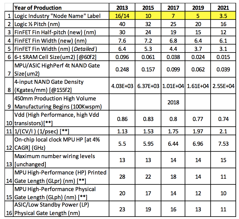
3nm is the physical size of the smallest dimension in the features in the chip. In 2017, the current 'node' is 7 nm. In this node, the dimension of the 'FinFET Fin Width' is 4.4 nm. [0]
It's fucking amazing to think that such microscopic features are repeatably produced at all, let alone at the scale of modern semiconductor fabrication. They can deposit layers of material measured in atoms. As in, 'Now I want a layer of copper 4 atoms thick' [1].
This table shows the actual measurements of the features of a device for each node:
Correct me if I'm wrong: no one is selling any 7nm chips right now, and no one is even selling 10nm chips right now, and no one will before the end of 2017.
So I don't think the answer is really that simple and straight-forward.
EDIT: I was wrong, Samsung is manufacturing commercially available SoCs on its "10nm" process. But in my defense, it's comparable to Intel's 14nm process.
One wonders how long 3nm chips will operate. Electromigration becomes a more and more serious problem as features get smaller and you can't afford to lose many atoms from a feature. This is worse for devices that are electrically active doing something; an idle flash drive doesn't suffer from this.
Will it be possible to fab a CPU at this density, or just memory devices? With memory, you can use error correction to compensate for faults. That's hard to do in logic. (Not impossible; it's been done, with CPUs that have self-checking. IBM has done that in their mainframe CPUs.)
At some point, the feature size stopped being a measurement of any specific feature on the IC, and just a generalized metric.
But ya, I mean if you forced them to, their engineers could probably produce the formula that mixes together a bunch of actual physical feature sizes, and explain why 3nm is not a lie - but its very much a marketing thing.
One obvious hint at this is how the different manufacturer's 'x' nm nodes have obviously different performances.
I'm reminded of the days of CDROM speeds, when at one point, 2X, 3X, 4X, etc. described an actual multiple of the baseline 150 KB/sec performance. Eventually, the number started measuring only the peak theoretical speed of reads from the outer edge of the disc. It ceased to be a meaning comparative measurement and pretty much became a version number.
That was for a completely different reason. CDs had Constant Linear Velocity (CLV). This means the disc would spin lower when the head was on other tracks, and faster on inner tracks, so that the same amount of data would pass under the head every second. This was a-OK until 8x or 16x and became really insanely pointless around 24x - with the disc being vigorously accelerated and brakes as the head moved from region to region.
At some point some manufacturer rightly decided “to hell with this idiocy” and made a CAV unit - Constant Angular Velocity - the disc would spin at Always the same rate, and if this means outer tracks read faster than inner ones, well, who cares.
The whole industry soon followed - there was no point in staying CLV.
I still have a 52x drive in an old PC. It will always take about 5 seconds to spin to max (sounding like a jet takeoff), even if a single sector needs to be read from it.
A neighbor of mine actually had a disc explode in his drive.
I couldn't believe it at first, but sure enough, the drive sounded like a maraca when I shook it.
My Diablo II disk shattered in my mothers PC when I was in the 7th grade, we were both rather upset (me because I lost my game disc in the era they were still used for anti-piracy, her because she needed to buy a new CD drive).
At this point a measure based on some number of average gates per square millimeter (won't that be fun to get everyone to agree to) would be better advertising, and more truthful.
Working on an areal density works better in an era where improvements are going closer to linear.
Aren't transistor densities vastly different for DRAM cells and logic? So you must choose what kind of stuff it is before "gates per mm^2" makes sense, no?
Different types of gates use different amounts of silicon area. Combining gates "cancel out" different number of transistors. So the gate density you'll end up with also depends on your specific application.
I think the number of transitors per unit area would be better. Though advanced applications mess with transistor sizes too, the situation would be better than gates.
why not just use more millimeters. if you don't invest $BNs in making smaller dies you can just sell bigger chips. and also charge more for a BIGGER and BADDER chip every year. then when it gets out of hand use a smaller process intel has abandoned already.
Price is proportional to die size. Processing one wafer is a fixed price, so the more chips you can fit on one wafer, the cheaper each individual chip.
Additionally, the number of defects is proportional to the area. The bigger your chip, the more chips you will have to throw away because of defects. E.g. say you have one defect per wafer on average, if your chip takes up the whole wafer, you will have no good chips. If you can fit 100 chips on one wafer, you will have 99 good ones and one bad one.
Correct me if I'm wrong, but I don't think AMD physically swaps out defective cores. I believe they're disabled individually in some kind of firmware. That's effective because the interconnect region is significantly smaller than the core area (and possibly made more reliable through feature size manipulation?). I think this has been standard practice almost dating back to multi-core introduction, where they sell high end multi-core chips as low end with some cores disabled.
AMD are shipping multi-chip modules with ThreadRipper (with two die) and EPYC (with four), and then because they are separate die you can trivially swap them out.
i believe this is a way for them to maximise yield, say their threshold is at least 3 dies must be good, and only 1 can be passable, then when they do tests and only 2 are good, they can swap out one of the passable ones, they can also rate the cpus differently too, they could also just swap out dies when all fail the test, i.e with threadripper and replace with another 2, then rate those.
   Today we are @ ~ 14, 16 nm.

   When we get to 7nm,  the today's chip that is using 1 cm^2 size silicon can probably be build with 0.25 cm^2 size silicon die.  (IO pads are another factor).

   If "everything (mainly yield?) being equal ", they should be able build 4x amount of chips from the same silicon wafer.   Again, assuming IO is not an issue.

    If the process cost, yield is similar, the new chips "can be" 4x cheaper OR they can pack 4 times # of transistors into the same 1 cm^2 area.   It can means more CPU, GPU cores, much larger L1, L2, L3 cache for the same chip size.


   When we get to 3 nm, they can build 16x amount of chips from the same 12 inch wafer.
Or pack 16x amount of transistors into the same silicon area.
A good example is:
   * Apple A10:  https://en.wikipedia.org/wiki/Apple_A10

   16 nm:   die area of 125 mm2, 3.3 billion


   * Apple A11: https://en.wikipedia.org/wiki/Apple_A11

   10 nm:  4.3 billion transistors[6] on a die 87.66 mm2
Small die = more chips per wafer. More transistors = More CPU cores, GPU cores, etc.
So nm is definitively has REAL impact on cost of a chip and amount of features (transistors) one can pack into a silicon die. It is not a simple marketing term.
When we get to 7nm, the today's chip that is using 1 cm^2 size silicon can probably be build with 0.25 cm^2 size silicon die. (IO pads are another factor).
If "everything (mainly yield?) being equal ", they should be able build 4x amount of chips from the same silicon wafer. Again, assuming IO is not an issue.
If the process cost, yield is similar, the new chips "can be" 4x cheaper OR they can pack 4 times # of transistors into the same 1 cm^2 area. It can means more CPU, GPU cores, much larger L1, L2, L3 cache for the same chip size.
When we get to 3 nm, they can build 16x amount of chips from the same 12 inch wafer.
"When we get to 3 nm, they can build 16x amount of chips from the same 12 inch wafer."
That's only if they are not up against pad-limited die size. Long ago people were running up against the issue of pad-limited die size, where the size of the I/O ring set the die size while the core logic ended up using less than all the available area. People were trying to figure out what extra stuff to throw into the core since it was shrinking so fast and the I/O was not. That was usually more memory, but that wasn't always useful.
So what's happening on that front these days? Are the current architectures actually able to make use of many more cores and memory without blowing up the I/O count of the chip?
But the OP asked if 3nm to 10nm is an apples to apples comparison, or if they are instead measuring something different for marketing reasons. In other words: will this "3nm" tech pack 11 times as many transistors as the 10nm tech for the same area?
you get to a point where the packaging costs as much as the die, then it doesn't matter how small it gets, you're just recouping the R&D for a smaller manufacturing process.
Feature size was always a measure of precision. It's just that one used to be able to draw artifacts 1 feature wide, while doing that nowadays seems to be useless.
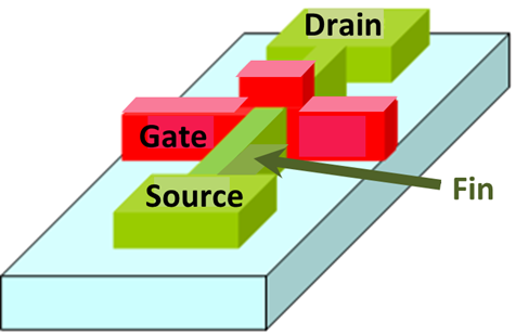
Just as a comparison, the Bohr radius of an doping election in a silicon crystal is around 10nm. I don't think you will see 3nm wide transistors unless they are fin-fets.
Imagine graph paper with the length of the side of a square being the feature size. 3nm. Where you shade in represents the metalization. Now imagine you have a design rule that says a metalization trace must be no less than 3 squares wide, for the sake of functionality.
That's a 3nm process. You might get away with putting to 9nm lines within 3nm of each other, or you might come up with some interesting transistor shapes that would not be possible on a larger process. But a trace would still have to be 9nm.
The problem is there are different parameters and it's possible to manipulate numbers. As far as I understand, what really matters is transistor density, and it obviously can differ for different processes even with same number. Intel of course claim they are better than others on the same numbers (see, for example https://www.extremetech.com/computing/246902-intel-claims-th... )
At 3nm, you get smaller than a biological protein and have features with countable numbers of atoms. And as far as my education went, quantum effects start to dominate, and bulk material properties start to (mis)behave very differently.