> Known good die (KGD): chiplets can be tested before assembly, improving the yield of the final device
Problem:
  > In general, a killer defect is defined as a defect that is 20% the size of the fabrication node.  For
  > example, a defect that is less than 9nm may be acceptable for the 45nm fabrication node, but a defect
  > larger than 2.8nm would be defined as a “killer” defect for the 14nm fabrication node.  For the 5nm
  > fabrication node, a defect measuring only 1nm could be a killer.
  >
  > This is one of the primary reasons that it has become increasingly difficult to yield large monolithic
  > ICs (as measured in die area) when using leading edge fabrication process technology
Solution: I understood it from the visual explanation in the first chip image (AMDArt2 png) and its description in this article:
The issue that you seem to be skirting around but not mentioning is, the chance a chip has a defect increases with die area since defects are randomly distributed across the surface of the wafer. Chiplets are a way for manufacturers to practically increase die area while keeping yields high.
In case it's not obvious the implication is that cost per good part starts to go up quickly. The wafer size and cost is essentially fixed so bigger dies mean both a lower % of parts are good and also fewer fit on the wafer in the first place. Wrong kind of hockey stick chart.
Is silicon manufacturing done entirely in a vacuum yet?
Because a vacuum pretty eliminates dust - with no air, dust just falls towards either the ground (if it is uncharged), or towards a positive or negatively charged surface (if the dust particle itself is charged).
No (at least not entirely: some steps are done in a vacuum or very low pressure), in part because it's harder to get a vacuum than clean enough air. Also it would cause a lot of other problems as well as not solving the whole problem: a lot of processing steps involve applying chemicals to the surface of the wafer, washing off those chemicals, or otherwise handling liquids which would boil in a vacuum. Those chemicals (including just plain water), also carry the same risk of introducing 'killer particles', so they are also a big part of the process control needed in a fab (the levels of contaminants in water that is required on modern process nodes is actually lower than can be detected practically with current technology: the last levels of water purification are effectively done blind, with yield as the only feedback mechanism).
Moore’s law is alive but the benefits are diminishing.
Until 2005 or so, shrinking transistors automatically increased speed and reduced power consumption. When that ran out of steam, the industry went to multi core and massive parallelism with GPUs.
Until recently each shrink also lowered the cost per transistor, but that seems to have run out also and has something to do with why Intel was stuck at 14nm for so long and why new GPU prices are so insane despite a collapse in demand and resolution of the supply chain crisis for high end chips.
Chiplets at best are neutral with regard to cost. If manufacturing overhead is low, two chiplets give you twice the transistors at twice the cost. The industry did not pursue chiplets with a lot of vigor until now because it was a less competitive approach to scaling than shrinking transistors until now.
I've been jesting for years that it should be referred to as "Moore's business plan", except it isn't a joke.
That business plan is no longer functional for Intel. Translated, Moore's business plan was to shrink die size, and speed up clocks, so much as to obsolete their previous offering with an 18 month half life.
It just doesn't work that way anymore, and hasn't for quite some time.
Engelbart's Scaling Observation[0], on the other hand, remains quite interesting, and from what I see remains in force. Genetics in particular is still pulling exponential gains out of the luminiferous ether.
Something to consider is that smaller chiplets have higher yields than monolithic dies given the same defect rate, which can certainly have an effect on price.
Right, more precisely cut out the defects from a wafer and save as much precious top-tier silicon as possible. Plus, another benefit of chiplets is that not every circuit needs the same performance level. Save the 5nm stuff for "hot paths" and use increasingly older processes for less performance/power critical applications, because while they might take up more space, they won't unnecessarily take up more next-gen fab time. Phones are literally the smallest and most power-limited devices we use so it makes sense to make every chip in them 5nm. Laptops and desktops and servers are not so constrained.
The problem is that GPUs are mostly underutilized outside games and machine learning, because the industry still hasn't moved away from the concept only a few selected group of developers can enjoy tooling to program them.
So everyone that works in other domains, without access to libraries written by the GPU druids, largely ignores their existence.
You can have compute shaders in WebGL2, and WebGPU is around the corner. GPU power is available but then you run into the thorny issue of specs...
Consumer machines vary wildly in their GPU capabilities, especially VRAM. So how do you know that your nice accelerated algorithm is going to work if the user has an old GPU? And what do you do if it doesn’t work? Run on the CPU? Tell the user their machine is too weak?
Here the advantage of GPUs (performance) is also the biggest disadvantage: a gigantic range of performance profiles. At least with CPUs the oldest CPU is only going to be a small integer factor slower than a new one in single thread.
What unites gamers and machine learning is an expectation that the user has a reasonably recent and capable GPU. But these are small, self-selecting populations.
On the server side the issue is cost. GPUs are expensive, and usually not necessary, so nobody is going to write code that requires one without a good reason.
Can you blame them? I just built a nice custom PC for my Son, with an 6 core cpu (with graphics, a ryzen -g class) 32GB of ram, 1TB NVMe hard drive, nice case, etc.
That cost about the same as a single mid-range video card. (Nvidia RTX 3070)
Why on earth would you add a requirement to your software/workflow that doubles your cost, and is just about impossible to find in stock?
I remember building my own PCs back in the 90s and early 2000s. In 2022 I don’t think any of my kids has ever even seen a desktop computer. It is all laptops, tablets, and phones.
I thought most generic computation workloads are ill-suited for GPUs. A normal web SaaS application is full of if branches and JMP instructions. Running this on GPU would slow it down, not speed it up.
Exposing GPU programming to anyone besides C, C++ and Fortran developers would already help, even if that would take a speed bump, as proven by the few attempts targeting PTX.
Pytorch isn't just for ML, it can do normal signal processing or physics too. The julia libraries for cuda and roc and oneapi also are general enough for those uses and approachable. Both can fall back to cpu without much modification to the rest of your code.
If you aren't doing signal processing, physics or something that would benefit from simd, then the gp is correct, a gpu won't do much for you.
That said people are always discovering algorithms that get better performance than you'd expect from new hardware.
For instance a frightening amount of CPU is spent in financial messaging systems on validating UTF-8, parsing XML and JSON, converting numbers written in decimal digits to binary and things like that. You'd think these are "embarrassingly serial" problems but with clever coding and advanced SIMD instructions such as AVX-512 they can be accelerated for throughput, latency, and economy.
The benefits of the GPU are great enough that you might do more "work" but get the job done faster because it can be done in parallel.
For instance the algorithms used by the old A.I. ("expert systems") parallelize better than you might think (though not as well as the Japanese hoped they would in the 1980s) despite being super-branchy. Currently fashionable neural networks (called "connectionist" back in the day) require only predicated branching (which side of the ReLU are you on?) but spend a lot of calculations on parts of the network which might not be meaningful for the current inference. It depends on the details, but you might be better doing many more operations if you can do them in parallel.
Given that GPUs are out there and that so many people are working on them I think the range of what you can do with them is going to increase, though I think few people will be writing application logic on them directly, but they will increasingly use libraries and frameworks. For instance, see
IME simd very rarely gets used by the compiler or runtime unless you make some slight changes in your data structures or flow, that require specific knowledge of the simd hardware. Asking a compiler to target unknown GPU architecture seems more likely to slow execution than speed it up. Even when writing my own cuda kernels I sometimes realize that something I am doing won't work well for a particular card and it is actually making me slower than the cpu. I'm sure we'll get there, but cards will have to converge a bit.
The point stands, the vast majority of workloads are unsuited for GPUs, either because they are full of divergent branches, or because the data transfer and synchronization overheads would cancel any performance gains.
For one thing, most employers will refuse to issue a laptop with a real GPU to developers and other employees because they are afraid they will get used for games.
That’s clearly untrue. Employers source computers from a few selected vendors and generally issue computers with average specifications because they can buy them in bulk and they are good enough. You can get a laptop with a more powerful GPU at most place if you actually need one.
No one is scared of employees gaming. Employees can’t install applications themselves on their laptops at most place.
That seems like a stretch? Isn’t the more obvious explanation that laptops with a real GPU are much more expensive and that the weaker, integrated GPUs are more than good enough for the vast majority of business use?
Today’s iGPUs are fast enough comfortable run plenty of games.
I have work provided high-end POS Dell Precision engineering laptop. It has an Nvidia discrete GPU, but I don’t think I’ve ever actually needed its power, and I’d gladly trade it for a laptop without…
The tooling is getting better. Debuggers are a thing now. You can program them in freestanding C++ with a little determination. Openmp target regions are friendlier syntax. Julia and a bunch of python machine learning things have GPU backends. They're still niche but slowly we make progress.
And the worst thing is that if execs etc. think that they can sit back down and breathe easy because they have a path towards even more infinite money in their chip business now that Moore's law isn't constraining that anymore, real R&D investments into actual advancements might not get the same attraction anymore...
The reason Intel was "stuck" at 14 nm was because it took Extreme ultraviolet lithography (EUV) many years longer to become viable than was predicted. Prices may have more to do with the EUV market being dominated by ASML which has serious trouble producing lithography machines fast enough to meet demand.
No, Intel was "stuck" at 14 nm because they believed that they will succeed to scale down the transistor sizes a lot more, without using EUV, as Pat Gelsinger has just explained in a long interview in the Verge.
However they failed to implement with good results the methods that they had hoped to work, while the others, i.e. TSMC and Samsung had much more realistic roadmaps, which added EUV at the right moment.
Intel was not stalled by waiting for EUV, on the contrary they were not prepared for the transition that was necessary when EUV was eventually ready.
If progress continues then they will need some other expensive machine. Either that or they’ll try to stretch the life of EUV the same way Intel tried to delay EUV with extreme multiple patterning.
It seems to me though that the ASML machines ought to get some competition from something more like a free electron laser.
> If manufacturing overhead is low, two chiplets give you twice the transistors at twice the cost
That doesn't take into account yields. One chip with twice the transistors is physically larger than two chips with half as many, and more likely to have a defect during production.
GPU prices are so insane because shareholders must make money, because NVDA miscalculated the crypto demand and doesn't want to hold the bags again (cf gtx 1060), and because NVDA artificially limited the supply of [rtx 30xx] cards.
> However, as it has in the past, the semiconductor ecosystem is adapting and as Chiplet technology builds traction, we will very likely see a period of accelerating innovation and new market opportunities opening as we move forward.
The whole premise is that chip innovation (and overall computing power) is continuing to accelerate, even though "Moore's Law as we've known it" has ended
I'd say that the premise of the article is captured in the title perfectly. One needn't to read the article to get it. So, we can strengthen your assertion and to say that "lotta people here are not reading the title." People react to the first part of the title. Seems they are really exasperated by all these repeated deaths of Moore's law.
Wouldn’t this mean that we should focus on writing more efficient code than before?
Especially in the startup space I saw companies building software with the hypothesis “users need the latest device for our product and they will get faster anyway so we don’t need optimize our code. Instead we deliver features on max speed skipping optimizations and wait until our users upgraded to newer devices during the coming 2-4 years”.
It’s offloading the cost to the customer. It is way cheaper to develop in some famous interpreted language than creating a set of robust compiled binaries. As long as customers can pay up for newer hardware we will keep seeing clunky UIs that can barely handle 20 list items of variable size without noticeable lag on a modern computer.
I don’t even blame the companies for doing this. The benefit to cost ratio of using idk C++ for everything is just too bad.
But the inefficiencies you sometimes see today can’t even be explained with any bad choice of language. You can create more than fast enough programs with interpreted languages with garbage collection. But then of course you need to know at least a little bit about data structures and not doing dozens of REST calls anytime anyone taps the screen.
Most code is so bad that "optimization" isnt the issue, at least in no sense that a language/runtime would help with.
It's just designed with O(N^3) architectures, "servers on servers" and "callbacks on callbacks", etc. because, seemingly, new features are made by very jnr developers -- who glue these idiot-proof frameworks together ---- trading needed-knowhow for polynomial behaviour.
Even if the Moore's law is not dead, single-thread performance and clock frequency have plateaued 10 years ago. This is the key factor. Because of heating even if you squeeze more transistors onto a chip you need to reduce the clock, so even if you may get higher computational throughput the latency will go down. And this is another argument for chiplets or any other alternative computational architectures.
It's amazing how often this is parroted. Anyone with a passing familiarity with the numbers knows this is actually not true at all.
Better caching, branch prediction, plus vast amounts of SRAM. There's been a slow & steady increase in the vast variety of single threaded workloads grouped together by "instructions per clock."
Both at the peak of the voltage frequency curve for workstations & overclocking, the apex of the optimization curve for data centre, and especially at the bare minimum for mobile devices with idle workloads.
Yes, it's a small fraction of the old days. It's still double in 10 years.
And as anyone who's migrated from an Intel Mac to Apple Silicon knows, "merely doubling" is a LOT.
Sorry, doubling in 10 years vs doubling in 18 months effectively is plateauing! Especially since it isn't really a consistent 10% growth per year, but a decelerating growth over that decade. Furthermore, much of the purported single thread performance is taken from a small set of benchmark tests, and so chip makers just optimize them for those tests. Generic single thread performance has undoubtedly not doubled in that 10 years.
In any field of any kind except probably silicon, 100% growth in a decade would be marvelous. I don't think anyone could call it a plateau.
> Furthermore, much of the purported single thread performance is taken from a small set of benchmark tests, and so chip makers just optimize them for those tests
"Single thread" is a notoriously difficult benchmark to quantify. Instruction queue depth, floating vs integer, branching vs linear, there are so many variables.
Passmark is fine. Workload simulation is state of the art.
Have clock speeds really plateaued? Sure it’s not “double every 18 months”, but in mid 2018 I bought an Intel 8700K that turbo’d to 4.7GHz and could (with liquid metal, dark magic and luck) overclock to exactly 5GHz. I remember people saying progress was slowing down, that we might not make it to 6GHz.
4.5 years later and Intel is bragging that their upcoming topline CPU will run 6GHz stock. I suppose one could call this a plateau compared to the good old days of the 80s and 90s, but it’s definitely still progress.
In late 2000, Intel promised that Pentium 4s will hit 10GHz by 2005 – on a presumed 130W power budget –, after the last 5 years saw clock speeds increase from 150MHz to 1.4GHz for the P6 architecture (at a stable 30-40W power budget), and other vendors saw similar increases.
Over 20 years later, we're barely scratching the 6GHz barrier with an opportunistic turbo mode that isn't guaranteed to kick in, if your cooling isn't up to the task of dissipating a record-breaking 250W of peak power consumption.
Part of why that happens is Intel selling chips closer to the red line. You need cooling similar to what used to be exclusive to overclocking just to keep the stock CPU cool.
Yep. We're apparently finding out that it's mostly a waste of electricity to get an extra 5% performance due to how far outside the efficiency sweet spot chips are being pushed.
Not just Intel either. AMD has joined the game as of Zen 4, and NVIDIA's been playing it with their GPUs forever as well.
Zen 4 desktop CPUs appear to have (as expected) virtually unchanged single core performance, and maybe 5% reduced multi-core performance, on CPU-bound workloads by reducing the power limit to cut total power consumption -- by over a 100W reduction in the case of the new 7950X! Granted, Intel's been doing that forever -- reign in Alder Lake and its power consumption also comes way down, again for barely a performance hit in CPU-bound multi-core tasks.
-----
Enthusiast grade CPUs and GPUs are basically sold in the equivalent of a TV's retail "demo mode" now -- where a TV has max brightness, contrast and saturation that you'd NEVER use, but is intended to just grab a customer's attention as they walk by. Being pushed so far outside of their efficiency sweet spot just to get that extra 5% to "win benchmarks", when outside of specific use cases (and even if you actually need that 5%!) you're just consuming 50-100% more electricity for utterly marginal gains.
What a waste of resources! All so children (or people who still act like them) can feel better about a purchase as they argue on the internet over nothing worth arguing about.
If you truly wanted to maximize performance per watt, you'd pick a very different design more reminiscent of GPU's. But then single-thread and low-multi-thread performance would really suck. So it will always be a carefully tuned tradeoff.
Nope. Not even. Again, as the grandparent post stated, everything is being sold with the default configuration being redlined.
You absolutely can reign it back in to sanity, and get better performance per watt over the previous gen, and still be noticeably faster over the previous gen.
-- -----
With AMD, apparently we're going to see BIOS updates from board manufacturers to make doing that simple. Set it to a lower power limit in a few keystrokes, still have something blazing fast (faster than previous gen), but use 145W instead of 250W. Or go even lower, still be a bit faster than previous gen while using around 88W on a 7950X instead of the 118W a 5950X did.
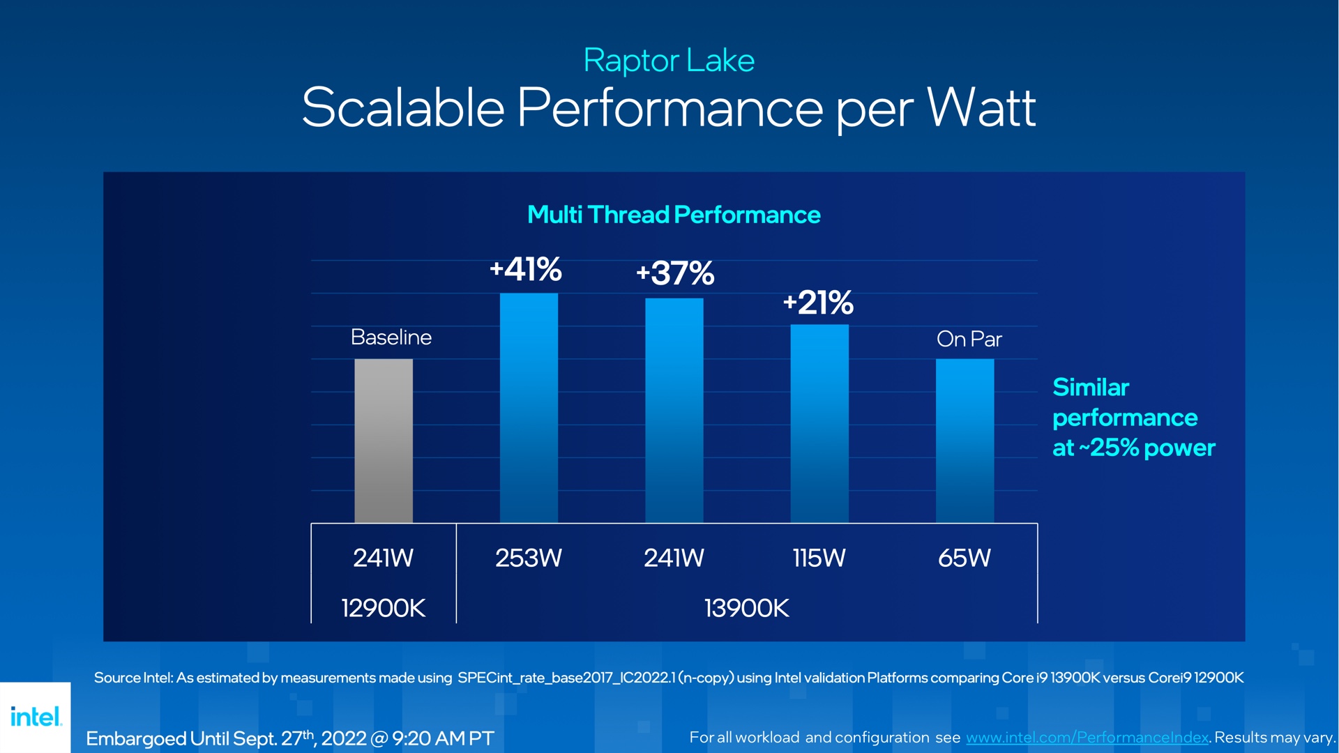
Intel -- who has been redlining their CPUs for years now -- even noted Raptor Lake's efficiency at lower power levels. Again, cut power consumption by 40-50%, for only a tiny performance hit. They actually made entire slides for their recent presentation highlighting this!
NVIDIA no different, and has been for years. Ampere stock voltages were well outside their sweet spot. Undervolt, cut power consumption by 20-25% and have performance UNCHANGED.
-- -----
Sure, there's more efficient stuff. Take last generation's 8-core Ryzen 7 PRO 5750GE. About 80% of the performance of an Intel Core i5-12600K, but only uses 38W flat out instead of 145W.
You don't even really need to rein it back, modern processors will throttle back automatically depending on how effective the cooling is. Anyway, the issue with manual undervolting is that it may adversely impact reliability if you ended up with a slightly substandard chip, that will still work fine at stock settings. That's why it can't just be a default.
>You don't even really need to rein it back, modern processors will throttle back automatically depending on how effective the cooling is
This isn't about thermals. This is about power consumption.
I'm not suggesting reigning in a CPU's power limits because it's "too hot".
I'm suggesting getting 95% of the performance for 59% of the power consumption. Because it's not worth spending 72% more on electricity for 5% increased performance. Again, even the manufacturers themselves know this and are admitting it. Look at this slide from Intel: https://cdn.arstechnica.net/wp-content/uploads/2022/09/13th-... Purported identical performance of previous gen at 25% of the power consumption. They KNOW the default configuration setting (which you can change in a few keystrokes) is total garbage in terms of power efficiency.
-----
I guarantee you server CPUs aren't going to be configured to be this idiotic out of the box. Because in the datacenter, perf/W matters and drives purchasing decisions.
Pentium 4 HT 3.8F, November 2004, 3.8GHz, 115W TDP
Core i9-13900KF, October 2022, 3.0GHz, 125W TDP
Of course, the latter does give you 8 performance cores and 16 efficiency cores so performance-per-watt has clearly improved; and it has 'turbo boost'. But in terms of sustained single-core performance? It's clear Intel's attention has been elsewhere. Such as on the laptop market, where power efficiency is king.
I'm curious if single threaded* games/applications that were CPU limited when the P4 originally came out run better on the 13900k with the same code.
That was my impression from games at the time, that they were coded with an expectation that clock speeds would keep going up in the future. But they didn't and the games probably run just as bad now as they did before.
And even in the Pentium 4 days, AMD CPUs managed similar performance as a Pentium 4 while running at lower clock speeds (which was a problem with some games that tried to auto-tune their performance-settings purely based on Pentium 4 clock speeds, even if you had an AMD CPU – thankfully at least in the Maxis/EA case, those settings were easily hackable, though, and could be easily adjusted to better match non-Pentium 4 CPUs, too).
the frequency plateau always been a power consumption/leakage thing, and power draw for recent intel cpus only reinforces that. it's probably too early to tell if 6ghz is a new normal
and fwiw ive had a 5ghz+ overclock on every cpu ive bought in the last ten years with a corsair 240mm aio, going back to the 3570k
I really hope there are breakthroughs that allow us to use other, trickier, semiconductors like GaN for chips, IIUC their efficiency could allow us to hit much higher frequencies for the same heat output. That said, I doubt we'd see 3nm processes for something like that.
IPC is still improving, so single thread performance is still increasing, even if clock speeds are not (at least not at the same as before). And new instructions (AVX ect) also help, especially if you can optimize and recompile your code.
It's at least enough that we have to take it into account:
We run our workloads across multiple Intel cpu generations and to be able to optimize utilization we have a "speedup factor" which is currently up to 1.7 for the latest generation we've tuned it for. And the base 1.0 performance is from Ivy Bridge, launched 2013.
It was basically a monopolistic warning from one of the founders not to release new products too fast so the company wouldn’t burn out. It worked. But it’s not some scientific or physical law and I hate when people refer to it as such.
/1999|2\d{3}/ - "Dirk Hohndel, who was then the chief Linux and open-source technologist at Intel, predicted that in 1999, Linux would penetrate the PC desktop market and displace Windows."[1]
Moore's Law is transisters per square mm or something like that.
Just drop a second layer on top with 3d fabbing and im sure moore's law will go on for a decade. inbe4 we have 2,4,8,16,32 etc layer architectures in the future.
If all you wanted was to deliver on the density you could just keep most transistors dark and still stay within the power budget. That's not very useful in general but maybe there are some aplications for it. AMD has been shipping their 3D VCache setup where they layer an extra cache only die on top of a CPU die. That's been benchmarking really well and is already an effective doubling that can be cooled with a normal PC setup. Maybe there's a few other tricks like that to get a few more vertical layers out of the same processes.
Unless I’m missing something, the article did mention Moore’s law proper with transistor density doubling every 18 months, but then meandered to talk about other things. M1 has 16 billion transistors thanks to TSMC. Each new node has delivered on Moore’s law with AMD and Apple. I don’t doubt that Moore’s law will stop. I can even say that it Moore’s law may have failed from time to time, but the spirit of the law lives.
Moving to chiplets doesn’t change transistor density. This is a packaging feature and not a fabrication feature. This is done for manufacturing cost reduction and yield improvements.
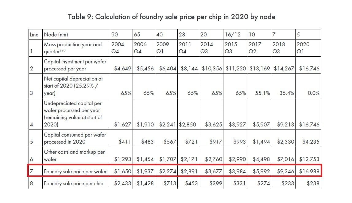
Folk haven't noticed however, because the "leading edge" logic manufacturers have 60% gross margins. The vast majority of their costs are in design, distribution and overhead.
Price rises of 30% to 100% have disguised that the cost of manufacturing the silicon is an order of magnitude more than a decade ago.
Granted, the above numbers are not the actual inflation adjusted wafer cost for leading edge nodes.
Most people believe Moore's law has already stopped on the density side. Jim Keller claims we have 50 more years of it at least. If it failed on the economic side only instead then the implications are very different. I do wonder if on the economic side of the law we are missing a bunch of innovation because every node step also reduced the number of players in the market. Right now on the bleeding edge there are only 3 players and that keeps trending down. They're also all ASML clients so we're pretty close to having a single monoculture in semiconductor fabrication. Maybe that's an inevitable result of the problem space but I do wonder if at least some of our lost efficiency comes from there.
Costs are rising by ~50% every cycle give or take.
Exponential growth is exponential growth.
They'll exceed the GDP of the United States in a few cycles.
The question becomes, when costs hit the ceiling that Apple is willing to pay, will TSMC still be able to front up with the good stuff and deliver the growth.
Obviously exceeding total GDP is not possible and we'll stop well before from just commercial considerarions as you describe. The question is how much of that is inherent to the problem and how much is lack of innovation. And we'll get to find out because if the processes stall from the economic side all the research turns to that whereas today it's an arms race for the next node and the increasing cost is taken as a given because as long as you get there the customers also arrive. Once that's no longer the case it frees up competitors from just chasing the node at equivalent costs to actually innovating on the total cost. If that leads to nothing then maybe we actually stop almost completely.
Tbh, it's less of a research problem per se, and more of an implementation one, in many ways.
The current pace of development is such that that they are plugging stuff in and hoping it works in LOTS of different ways.
A small army of electrical engineers work night shifts at TSMC as well, something Intel could never pull off given American labour market demand for EEs.
I suspect you're right, when costs have to come down timelines will blow out to something more reasonable.
One interesting point is that even if Moore's law stops or slows down, chiplets allow us to increase transistor count independently of transistor density. Thus keeping alive the spirit of the law (processors get more and more transistors).
I am not convinced moore's law no longer holds true, consider that there is a third dimension that no one has yet figured out.
I am no silicon engineer but I suspect a chip that fully takes advantage of the third dimension would be something like a sponge full of built in channels for the working fluid to remove heat.
First however I suspect you will see chiplets arranged vertically like heatsink fins and the whole cpu would effectively be the water block, basically a vlsi version of the cray 3
3D is already being used for ram/flash IC's. That's possible because most memory cells aren't being used in a memory chip - so heat density is reasonable.
3D is also used in AMD's 3D cache.
But 3D logic on logic is more complicated because of heat issues. AFAIK there's no workable technical solution for that yet.
Heat removal is basically a 2D problem. A 3D pipe has a 2D cross section in which fluid can transport heat. Right now we are mostly limited by heat removal, so adding more height to the chip doesn't help anything with the heat. Also, the chips are already many layers thick and each layer means processing steps which means time and money.
If you look into flash memory which aren't limited by heat, they have dozens of functional layers already and then we also stack those silicon wafers.
The history of computing is moving from one paradigm to another. We are well past the fast speedups in single thread transistor-based performance phase and into the hyper-parallelization phase.
3d stacking is another innovation that can help.
But I think within a decade or two there will be a move away from silicon-only transistors to something like memristors or some type of optical or optoelectronic system that hasn't even been invented yet. This will provide some iterations with again radical parallel interconnect and quite possibly single thread speedups.
> Obviously, given these data, volume is VERY important in business models that operate with high fixed and low variable costs.
Off-topic but I wonder how much cheaper mobile phones would be if the manufacturers did not have to come up with a hardware design update every year or so? What if mobile phones were built to last longer, which would reduce the cost per phone due to high volume? Of course, I am not suggesting this is good for business but as a mere thought experiment.
> With $100 million in funding, the IDEAS and POSH programs ... aim to combat the growing complexity and cost of designing chips, now approaching $500 million for a bleeding-edge SoC. Essentially, POSH aims to create an open-source library of silicon blocks, and IDEAS hopes to spawn a variety of open-source and commercial tools to automate testing of those blocks and knitting them into SoCs and printed circuit boards. If successful, the programs “will change the economics of the industry,” enabling companies to design in relatively low-volume chips that would be prohibitive today.
> OpenROAD is a front-runner in open-source semiconductor design automation tools and know-how. Our project reduces barriers of access and tool costs to democratize system and product innovation in silicon. The OpenROAD tool and flow provide autonomous, no-human-in-the-loop, 24-hour RTL-GDSII capability to support low-overhead design exploration and implementation through tapeout. We welcome a diverse community of designers, researchers, enthusiasts and entrepreneurs who use and contribute to OpenROAD to make a far-reaching impact.
> All the big EDA providers, as well as leading chip companies, are active contributors to ERI projects. In fact, Cadence, Synopsys, Mentor, NXP, Intel, IBM, Intel, Qualcomm, Arm, Nvidia, Analog Photonics, SRI International and Applied Materials all have contributed speakers and engineers or materials to ERI effort ... the key to getting industry players to accept open-source EDA is whether it makes the design process more efficient without breaking anything—and whether it is possible to extract decades worth of design experience from libraries of millions of existing designs and use that to spot errors in real time in existing designs.
Jeff Dean's recent talk on ML for hardware design seems like a great application of the tech in a space where we are seeing design process costs balloon (see https://www.youtube.com/watch?v=FraDFZ2t__A).
I was actually wondering if someone could explain where that cost increase is coming from. I know the design rules get more complicated as the process node shrinks, but I thought most of those design rules are essentially “taken care of”, because customers use building blocks from the foundry that already have those design rules baked in? And it’s still using the same software I thought?
a lot of it is that to get continued gains, you run out of easy stuff to optimize. when Moore was alive and well, the job of chip designers was to build abstractions that let them cheaply scale down their designs without introducing too much overhead. now, is you want to announce 30% gen on gen improvement, you can only count on the fab to give you half of that (and even that has gotten harder. co-optimization is now needed, but is really hard). for the other half, you now need to hunt down every last inefficiency that you previously accepted to make your life easier. pure digital signals go to pam4. layout becomes less regular. you start trying to optimize the whole chip rather than just combining optimized pieces. then in 3 years, you have to find another 15% and the process repeats, but this time you have used up all the low hanging improvements.
https://en.wikipedia.org/wiki/Chiplet
This seems to be about the third reason listed:
> Known good die (KGD): chiplets can be tested before assembly, improving the yield of the final device
Problem:
Solution: I understood it from the visual explanation in the first chip image (AMDArt2 png) and its description in this article:https://www.nextplatform.com/2021/06/09/amd-on-why-chiplets-...