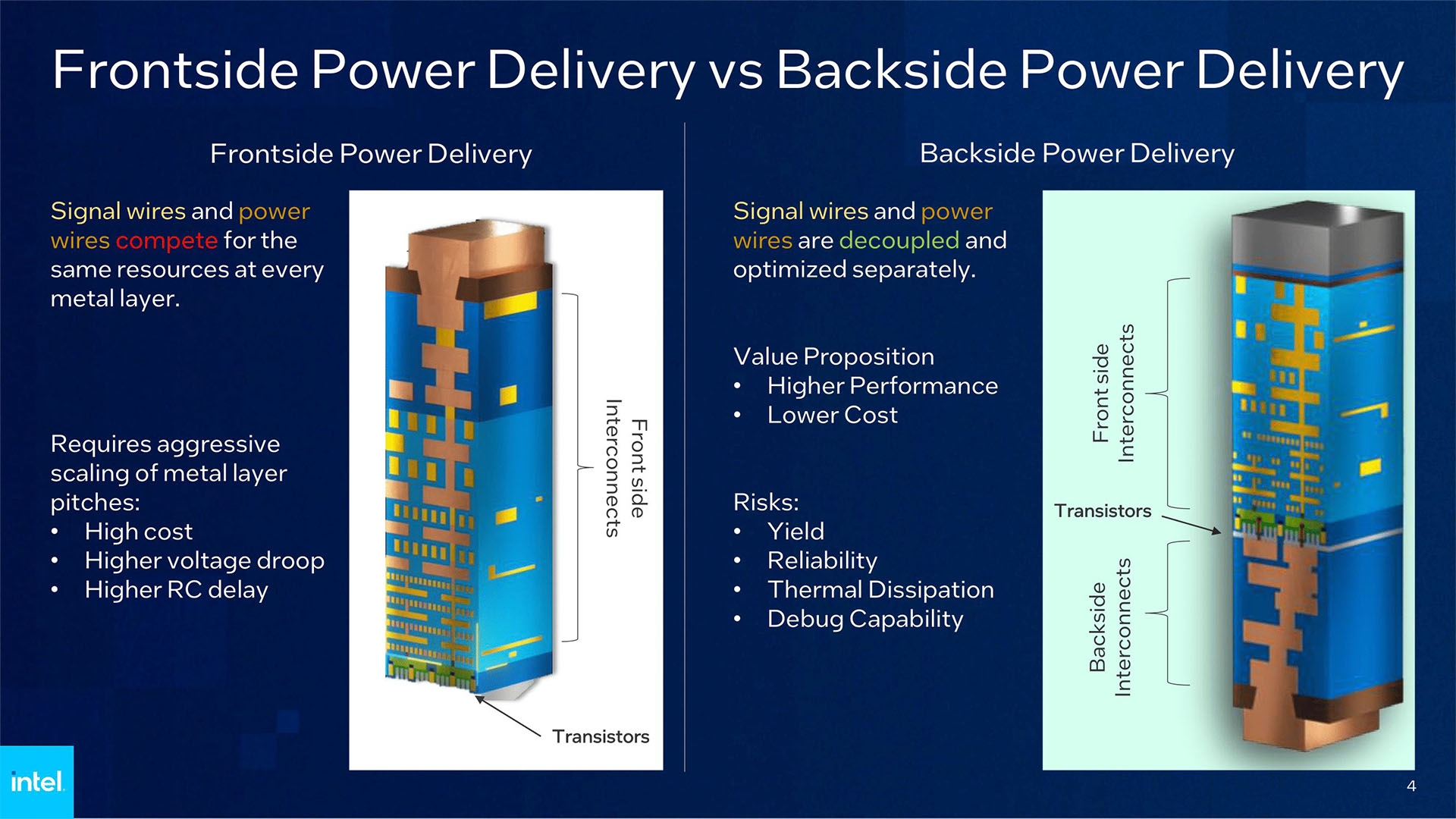
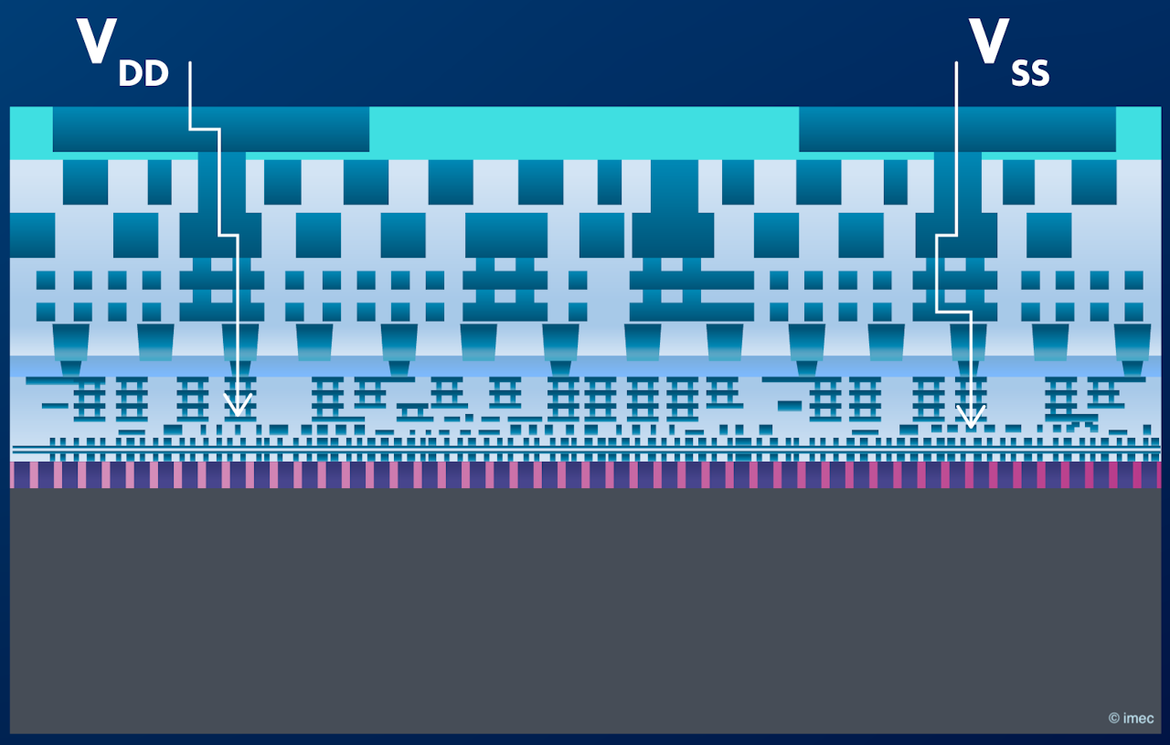
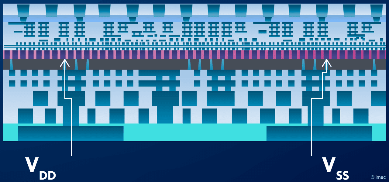
ICs are manufactured on silicon disks called wafers. Discs have two sides, and traditionally, everything was done on top. We can now do power on the bottom. This makes things go faster and use less power:
* Power wires are big (and can be a bit crude). The bigger the better. Signal wires are small and precise. Smaller is generally better.
* Big wires, if near signal wires, can interfere with them working optimally (called "capacitance").
* Capacitance can slow down signals on the fine signal wires.
* Capacitance also increases power usage when ones become zeros and vice-versa on signal wires.
* Big wires also take up a lot of space.
* Putting them on the back of the wafer means that things can go faster and use less power, since you don't have big power wires near your fine signal wires.
* Putting them in back leaves a lot more space for things in front.
* Capacitance between power wires (which don't carry signal) actually helps deliver cleaner power too, which is a free bonus!
This is hard to do, since it means somehow routing power through the wafer. That's why we didn't do this before. You need very tiny wires through very tiny holes in locations very precisely aligned on both sides. Aligning things on the scale of nanometers is very, very hard.
There's still the question though of why they didn't do this decades ago - seems very obvious that this layout is better. What changed that made it possible only now and not earlier?
My knowledge isn't current enough to offer more than speculation.
However, something like an 80286 didn't even require a heatsink, while my 80486 had a dinky heat sink similar to what you might find on a modern motherboard chipset. At the same time, on a micron node, wires were huge. A few special cases aside (DEC Alpha comes to mind), power distribution didn't require anything special beyond what you'd see on your signal wires, and wasn't a major part of the interconnect space.
Mapping out to 2024:
1) Signal wires became smaller than ever.
2) Power density is higher than ever, requiring bigger power wires.
So there is a growing disparity between the needs of the two.
I suspect in 2000, this would have been basically restricted to $$$$ military-grade special processes and similar types of very expensive applications. In 2024, this can be practically done for consumer devices. As costs go down, and utility goes up, at some point, the two cross, leading to practical devices.
I suspect a lot of this is driven by progress in imagers. There, the gains are huge. You want a top wafer which is as close as possible to 100% sensor, but you need non-sensor area if you want any kind of realtime processing, full frame readout (e.g. avoiding rolling shutter), or rapid readout (e.g. high framerate). The first time I saw 3D IC technology in mainstream consumer use were prosumer-/professional-grade Sony cameras.
I have strong fundamentals, but again, I stopped following this closely maybe 15 years ago, so much of the above is speculative.
"Better" is relative, the layout introduces more fabrication steps so it's only better if you actually get some benefit from it. Decades ago designs didn't require as much power or have as many transistors to wire so it wasn't an issue.
You might as well ask why, since we can do it now, Shockley didn't simply start at 3nm. It's all a very long road of individual process techniques.
> You need very tiny wires through very tiny holes in locations very precisely aligned on both sides.
Key word here is "both sides". It has challenges similar to solder reflow on double sided boards: you need to ensure that work done on the first side isn't ruined/ruining work on the second side.
"The challenges with BPR are that you need a low resistance and reliable metal line that does not contaminate the Front End Of Line (FEOL). BPR is inserted early in the process flow and must stand up to all the heat of the device formation steps."
Contamination = metals used musn't "poison" the front-side chemistry. So they end up using tungsten rather than the more usual aluminium. (Copper is forbidden for similar chemistry reasons)
It also (obviously) adds a bunch of processing steps, each of which adds to the cost, more so than putting the rails on the front side.
I think it's more that it's only necessary now. It's such a pain to make that you'll only do it given no other option. A lot of what modern processes are going was possible ages ago, but it was basically always better (in terms of ease for performance gain) to go smaller instead. Now that smaller doesn't help so much, you can see them pulling out all the other tricks in the book to try to improve (and costs going up as a result).
> You need very tiny wires through very tiny holes in locations very precisely aligned on both sides. Aligning things on the scale of nanometers is very, very hard.
Do you need to align that precisely? Can't the power side have very large landing pads for the wires from the signal side to make it much easier?
The wafer is thick. Let's call it a mm thick (not quite, but close). Devices are tiny. The claim is 1.6nm, which isn't quite true, but let's pretend it is, since for the qualitative argument, it doesn't make a difference. That's on the order of a million times smaller than the thickness of the wafer.
Historically, everything was etched, grown, deposited, and sputtered on one side of the wafer. The rest of the wafer was mostly mechanical support. The other side of the wafer is a universe away.
The world is more complex today, but that's a good model to keep in mind.
For a 3d integrated circuit, you would do this, and then e.g. grind away the whole wafer, and be left with a few micron thick sheet of just the electronics, which you'd mechanically place on top of another similar sheet. That's every bit as complex as it sounds. That's why this was restricted to very high-end applications.
As for whether the wafer is a huge ground plane, that's complex too, since it depends on the top of the device and the IC:
* First, it's worth remembering a pure silicon crystal is an insulator. It's only when you dope it that it becomes a conductor. The wafer starts out undoped.
* Early ICs had the whole wafer doped, and the collector of all the NPN transistors was just the wafer. There, it was a ground plane.
* SOI processes deposit a layer of glass on top of the wafer, and everything else on the glass. There, the wafer is insulated from the circuit.
So all of this can very quickly go in many directions, depending on generation of technology and application.
I'm not sure this post is helpful, since it's a lot of complexity in an ELI5, so I'll do a TL;DR: It's complicated. (or: Ask your dad)
The level of purity and perfection there is a little bit crazy to conceive.
It's also worth noting how insanely tiny devices are. A virus is ≈100nm. DNA is 2nm diameter. We're at << 10nm for a device. That's really quite close to atomic-scale.
There are something like ≈100 billion transistors per IC for something like a high-end GPU, and a single failed transistor can destroy that fancy GPU. That's literally just a few atoms out-of-place or a few atoms of some pollutant.
The level of perfection needed is insane, and the processes which go into that are equally insane. We are making things on glass, but the glass has to be nearly perfect glass.
>> There are something like ≈100 billion transistors per IC for something like a high-end GPU, and a single failed transistor can destroy that fancy GPU.
No, it can't thanks to this fancy marketing strategy where you sell faulty GPUs at lower price, as lower-tier model.
can is important there. Not all failures can be masked off. And this only makes the slightest of dent in the level of reliability you need in making any given transistor.
The demand for perfection is mildly ameliorated by having a few redundant circuits and microcode and then a software layer that can detect and workaround defects. If your GPU loses one if its 1000 integer math units, it doesn’t die, it just slows down for an operation that might otherwise use that one.
> Typically, backside power delivery enables thicker, lower-resistance wires, which can deliver more power to enable higher performance and save power. Samsung's paper noted a 9.2% reduction in wiring length, enhancing performance
btw, you appear to be shadow banned, probably on account of being downvoted for making short comments like "good" or "I don't get it"
Short & simple responses may be adequate at times, but usually people will view it as not adding anything
Perhaps reviewing guidelines https://news.ycombinator.com/newsguidelines.html will give an idea of the ideal being yearned for (granted, it's an ideal). In general, trying to enhance the conversation with relevant information/ideas. "your links are 404" was definitely relevant here
Their new posts will be dead. You can enable seeing dead posts in settings. Then if you click on their account & view their comments, it'll all be grayed out
instead of signals and power path going through the same side (frontside) causing all sorts of issues and inefficiency, they're decoupling where power is coming from (from the other, backside, err side).
More importantly, intel saw it as one of two key technologies of them moving into angstrom era, and was touting itself they'll be the first one to bring it to life (not sure they did).. so this seems to be more of a business power move.
It looks like the topology for backside moves the transistors to the middle so "singal wires and power wires are decoupled and optimized separately" instead of "compete[ing] for the same resources at every metal layer"
So, if I understood that correctly, "frontside" actually is the top side, and "backside" is actually the bottom side. They're delivering power from the bottom (substrate) side, and connecting the data on the top side.
Half your wires deliver power, half deliver signal. So if you do both on the same side, you need twice the density of wires. If you split the delivery into two parts, you get double the density without needing to make things smaller.
This isn't quite right. Big wires (ideally entire planes) deliver power. Small wires deliver signal. Half and half isn't the right split, and you don't want to make power wires smaller.
The very different requirements of the two is where a lot of the gains come in.
It is going to get even a bit more interesting when you consider power gaters and virtual power supplies. Now the real power will be on the back side and the virtual power will be on the front side. Fun time for power analysis.
True! I went a little far in the name of 'eli5'. I think it roughly holds that you gain about a factor of 1.5 in routing density by removing the power distribution, so you can relax some critical patterning. But I havent looked closely in a long time.
Oft-missed pedagogical point for working with five-year-olds:
Precision is important. You'll notice every comment I made was as simple as I can make it, but /technically correct/. I did not oversimplify to where I changed facts.
* It's okay if five-year-olds don't fully understand something. That builds exposure, and leaves a placeholder for future information and curiosity.
* On the other hand, if you build out an array of misconceptions, those become very expensive to address later.
To a large extent, the younger the child, the more comfortable they will be with being told things they don't understand. A baby doesn't care if you're reading them a book on trucks or a book on homeomorphic transformations; they're picking out the phonemes. A toddler will trust you as an adult, and won't understand 90% of the stuff they hear anyways. A five-year-old, you can still say a lot they won't understand and they'll be not just okay but happy. By maybe seven, lack-of-understanding will become frustrating, and in most cases, by eleven, it's gone.
I could write a long essay on this stuff, and why it's so important to maintain that ability to be confused and half-understand, but I very intentionally leave placeholders when working with five-year-olds.
The scientific litterature and IPCC’s summaries warned about these phenomenon.
When 2 billion people will be living under wet bulb temperature that can’t be tanked by the body it’s going to be a mess worldwide.
People who live in the humid tropics are already on a knife's edge. A small increase makes the heat intolerable and you will see either mass death or mass waves of immigration. "Just build aircon" doesn't work when you're talking about people with intermittent (or no) electricity and who have an annual income equal to a single aircon unit.
All the more reason to urgently develop the world to at least the level of Malaysia / Thailand (or ~Western Europe ca. 1950). If we quit fossil fuels cold turkey it is those very same people in the tropics that will starve. But making that connection requires thinking about second order effects, a tall order for the degrowth cult.
I want to continue growing, just replace fossil fuels with renewables or nuclear in all developed countries, and subsidize the same for poor countries who haven't historically emitted much and don't have the wealth to transition themselves. There isn't this false dichotomy of degrowth vs growth. We can grow our economy without growing emissions.
The medium-term problem for these hot countries is that extreme heat negatively impacts education and economic productivity. Whenever there's a heatwave (which will become more frequent) they have to keep their kids home. Worker producitivity is negatively impacted. It's terrible for their economic development. The US and Australia and Canada continuing to pump more fossil fuels instead of simply building renewables does nothing help the average person in Sri Lanka living under 30+ degree heat. It is actively physically harming them in a very real way. It's an indirect, diffuse form of physical assault.
The long-term problem for these hot countries is that wet bulb temperatures will make it literally uninhabitable unless you have electricity and aircon, which many don't. This is not a matter of if, it's a matter of when. If we keep emitting, temperatures will keep rising, until the point that this becomes true. It is causality.
I want conservatives to think about this latter point because the consequences are mass immigration to colder countries, primarily the US and in Europe. Then the side-effect of that will probably be a rise in authoritarianism in these colder countries as a reaction to the mass immigration. None of this benefits anyone.
Thank you for the response and sorry if my comment was excessively snarky. I think we share the same concerns and have the same goals and even mostly agree on practical steps to get there. I've just seen and heard too many degrowth advocates (that really want to return to 19th century economy with 21st century populations) recently and it's really worrying me.
> and subsidize the same for poor countries who haven't historically emitted much and don't have the wealth to transition themselves.
Yes! With a fraction of the money sloshing around various "charities" and NGOs, mostly spent on salaries, you could build solar with storage for millions of people. Of course in practice it would be really complicated, you have to make sure the right people run the systems and there will be bad cases of corruption. But it really is the least we could do.
> The US and Australia and Canada continuing to pump more fossil fuels
The funny thing is that the market is turning even Australia and Texas into solar superpowers. Ever since solar became the cheapest form of generation both have seen an incredible boom in solar, with almost no policy incentives. This is a huge win for the planet, if people want to build solar because the incentives align they will just do it without costing larger society any (political) capital.
> It is actively physically harming them in a very real way. It's an indirect, diffuse form of physical assault.
I follow the logic and agree about the causality chain, but this is a road it's best not to go down. It quickly turns into personally blaming people for things they had no control over. That has never been a good way to persuade people. Imo it's also a lazy deflection, since humanity has never really paid any attention to its resource usage. The only difference is that Industrial societies gained the capability to affect the planet on such a large scale.
> The funny thing is that the market is turning even Australia and Texas into solar superpowers.
I think the market is too slow by itself. There's a technical reason for this. Externalities are mispriced, causing market failure. Markets may get there by themselves eventually, but not as quickly as they should.
Australia is set to become a solar superpower partly because the center-left government got into power. The center-right is hostile to renewables even though Australia is perfectly situated. This wasn't always the case, the center-right used to be somewhat favorable to renewables until they got radicalized by the usual stuff.
Likewise with the US, the IRA's renewables provisions only got passed because the center-left is in power. Renewables will still grow with Trump in power due to state-level subsidies, but far slower than what would otherwise happen.
My primary concern with all this is this human, political side. Solving this problem is as much a persuasion exercise as a technology exercise. We need to somehow get the political right to drop their defenses. They are blinded by their dislike of lefties and Greta Thunberg and so on, that they are not thinking rationally about the objective market failure that needs to be corrected.
Further on this, we need to present a new narrative to the degrowthers. The degrowth left sees a mutually exclusive trade between growth and climate change. Which is sort of true if conservatives get in power and don't change their belief system.
What's needed is a sustainable growth narrative where you give conservatives their growth and you give the left their lower emissions. It is not that hard to implement if people could just stop being so politically radicalized.
Smol nit: immigration means moving into a country. In your example we'll see a lot of emigration, people moving out of the country. You emigrate from one country and thereafter you immigrate into another.
Even smaller nit: Isn't it basically two sides of the same coin in this context? I'm not sure what the intent was in the previous post, but it could just as well be from the perspective of someone living in a desirable country worried about a lot of immigration of less fortunate people.
My interpretation was that countries with growing cimate problems will start seeing more and more immigration, which is wrong. It'll see more and more emigration.