> Another striking advance is the migration in the P-core database from a 'sea of fubs' to a 'sea of cells'. This process of updating the organization of the P-cores substructure moves from tiny, latch-dominated partitions to more extensive and ever larger flop-dominated partitions that are very agnostic as things go.
I like to pretend I know a thing about CPU design, but I have to admit, I have no idea what's going on here.
Chip design is SUCH an advanced topic. It's potentially one of the most advanced human disciplines at the moment.
I have a friend[0] that is doing his Electronics Engineering masters in Germany (very prestigious engineering university) and they're studying a freaking Pentium 4. Even for them the cutting edge chip design is black magic.
Question: there's a lot of hands-on learning resources on the construction of a simple microcoded processor, or an in-order pipelined processor where the most headache-inducing thing you have to deal with is forwarding results – but is there one on the essential elements of "modern" superscalar OoO, e.g. the circuits that check for hazards and delay dispatching etc.?
It's not that it's magic I would love to learn about: it's that I'd like to know what happens behind the scenes when we say that (for example) "results get reordered in the reorder buffer"!
Modern chip designs have an enormous amount of logic and therefore standard-cells. And when you are dealing with a huge amount of cell all together, it quickly becomes unmanageable, syntheses tools runtime explode, quality of results declines, results become chaotic, ..
So chip designs are spliced into partitions. Each partition is a part of your design that you synthesized separately.
For example you may setup a partition for the core, and you can instantiate it multiple time into a core_cluster partition.
Note that: synthetiser's logical optimizer cannot work on logic across partitions, so you don't want to small partitions (otherwise you will have more manual optimize to do) but you also don't want too big partitions (otherwise runtime and development iteration time increase).
The question is what the good size for a partition ?
* ALU is ~ 10 K cells (synthesis runtime range from few seconds to ~5 min)
* small core (low-end) is ~1M cells (synthesis runtime range from 1~8 hours)
In the Intel terminology: "sea of FUBs" approach is to prefer small partitions, while "sea of cells" approach prefer big partitions.
About the predominance of latch or flop, it's mainly a consequence from the level of manual optimization. (latch are smaller, but harder to manage, and it give diminishing returns with new process node). Same for process-node-specific vs process-node-agnostic.
PS: Most modern designs are "sea of cells" according the Intel terminology
I read it as "fubs were small partitions, but now with the latch boundaries dissolved between fubs, the partitions are bigger (containing flops from many fubs)".
I look forward to the decline in interest in generative ML. There is a screaming need for secure online services to enable democracies to face off the threat from authoritarian regimes. To do this we need hardware that enables actors as in actor model with truly private state, not sandboxed where there is an external entity that can observe its state. Today pretty much all designs has a perverse von Neumann architecture where state is shared across different compute devices like network controllers and management engines. And the software stack is more of the same sandboxing. Apple includes a Secure Enclave on its SoC where you may only communicate with it by sending messages like a proper actor, but why aren’t servers made entirely of secure enclaves? If the memory of each enclave was private by design in hardware it shouldn’t be necessary to encrypt it.
How would that empower democracies more than authoritative regimes? The technologies you mention are means of control, and are used as such. Secure computing doesn't help you when the regime owns the keys (or can coerce them out of the vendor).
I may very much be wrong about it, but intuition and experience tells me that means of control usually empower authoritarian parties first and foremost, unless fully owned and operated by individuals - which, in computing, is very much counter the trend and the zeitgeist.
Good question and I don’t have a good answer. My intuition is that democracies are more dependent on transparency and that lower complexity and higher security would enable more distribution in control.
I intuitively agree on transparency being important for democracies, but then I see "lower complexity" and "transparency" as both being opposed to "higher security". Taking for example the secure enclave you mention, its whole point is to bolster security through removing transparency via a complex hardware and software system.
You (and probably a lot of tech nerds) need to remember democracy is a social challenge, not a technological challenge. What applies to technology does not necessarily apply to society.
The more opaque and complicated you make so-called "democracy", the less the electorate have faith that it is fair and representative. Simplicity and transparency is security, security that democracy is working in a way everyone can and must agree with even if they don't necessarily like it.
I don't think it's technology vs society issue (and I do honestly maintain that social problems are supposed to be solved by technology, because that's literally what technology is for by definition). It's an issue of framing security.
Cybersecurity mostly assumes the vendor is the trusted party - the users are the sheep the vendor is shepherding[0]. Security is designed to pretend first and foremost the vendor, and secondly its flock of users, against attacks from outside parties and other users. The users are untrusted parties here.
Democracy, in contrast, is an unusual relationship in which it's the organization - the government - that's the untrusted party. Transparency is crucial to security of this system, because the very party that organizes it is the one most incentivized to subvert it. It's a special case where opaqueness is not accepted. This is why it's hard to port ideas from cybersecurity to democracy - the assumptions underpinning the two are opposite to each other. Most of what infosec considers good practice would immediately violate the electorate's faith you refer to.
Exercise for the reader: how would our computer systems look if the security field emphasized end users as trusted, and vendors as malicious parties?
--
[0] - I love how the ubiquitous analogies to good shepherds, including biblical ones, conveniently omit the fact that the very reason shepherd cares for their sheep is so they can be fleeced for wool and/or slaughtered for meat.
AI slop is perfect for reducing usefulness of transparency: you can generate so much bullshit nobody will ever be able to discern what is worth looking at even if you can have access to everything. We aren't there... yet (but perhaps ask Google how is their search product doing in the past couple years). I'd love to hear what Shannon would have to say about this situation.
To be clear: It's not that the electorates like authoritarianism, they hate "democracy" which doesn't listen to them nor work for their interests and benefit.
but that's the whole point - the democracy has to consider interests of various group and - ironically - it only somehow works when you have a single unified group. When you have diverse groups - there interests do not align and it becomes a clownshow
Server-side secure enclaves (confidential computing) are becoming significantly more popular for the exact purpose of providing secure online services, and a decent number of companies are already doing this today.
There are technical challenges in using secure enclaves correctly, and those limit adoption. At Anjuna (anjuna.io), we are working on those problems and seeing good results for our customers.
The consumer needs Intel to get back to somewhere within reach of competitive semi manufacturing. Fingers crossed though the past decade doesn't inspire hope...
What a disaster! I hope this is the bottom, and that there's enough expertise left at Intel to save the company (and I guess enough political will in Washington to subsidize it).
Anyone got an estimate for when we might see new Thinkpads with these chips? End of this year? I'm not unhappy with my current gen 3 T14 but if I could have a device that's closer to my Macbook Pro M1 in performance and efficiency I'd be willing to upgrade, as I still like Linux much more than MacOS.
Not a Thinkpad and not Intel, but that already seems attainable with the asus G14 (AMD 8945HS + NVIDIA 4070) or the upcoming asus zenbook S16 (AMD HX 370).
Intel themselves claim 45 TOPS (IPC isn't a thing in NPUs) coming from their NPU. AMD didn't reveal the chip total of the new Ryzen series, but their NPU gets 50 TOPS. The only reason Intel's numbers are so much higher ("120 TOPS!") is that Intel included their chip total (what the GP dies can achieve, but at far lower power efficiency) with the NPU numbers, AMD doesn't include this. Presumably their GP cores would be able to achieve similar numbers.
Given that AMDs NPUs were already ~78% more power efficient than Intel's and both are claiming ~50% power efficiency increases, I'm not sure why there would be a big upset here.
Not really defending AMD here, but they have been investing hard into NPUs for about four-five generations now, while Intel only really hopped on the bandwagon last generation. Unless you just believe Intel has the best engineers in the world, period; there's no reason to believe they would close the gap that quickly.
Based on the instruction set extensions supported, the design of Lunar Lake has been started later that the designs of Arrow Lake and Arrow Lake S.
When first announced, Lunar Lake was supposed to be manufactured by an Intel CMOS process that will be available only in 2025 (18A).
At some point, Intel has decided to retarget Lunar Lake for the TSMC "3 nm" process, and it appears that this decision has allowed them to be ready for product launch much earlier, so it might be launched before Arrow Lake and Arrow Lake S (the latter of these 2 is a desktop CPU that will also be made in the TSMC "3 nm" process, according to rumors).
At Hot Chips 2024, Intel is scheduled to make a more detailed presentation of Lunar Lake.
Xeon 6E launched this week on the Intel 3 process. Benchmarks of production silicon look good for performance but especially good for performance per watt. Definitely competitive with AMD.
A lot of the efficiency improvments depend on the new thread scheduler in Windows 11.
I doubt these chips are going to be great or at least, as efficient in Linux as they are in Windows 11.
AMD going for Zen5 and Zen5 is exactly to avoid this issue and the need for complex scheduling algorithms.
I’m sure support for heterogeneous CPU scheduling will continue to improve on Linux too. Intel’s server chips have little cores too, and those servers are overwhelmingly running Linux, so they have a clear reason to continue to help support scheduling improvements in Linux as well.
Compared to the previous generation, scheduling should be easier. Meteor Lake has P Cores with SMT, E Cores, and Low Power E Cores. Lunar Lake just has P Cores (no SMT) and E Cores.
Anything RF is deep wizarding lore, a world filled with wonders unexplainable to laypeople.
The effect is well known, and the reason why if you open up your average phone, there will always be a ton of shielding around components. All the high speed buses can and do create lots of side emissions... so in order to allow a phone to function with its extremely tiny bunch of antennae in direct proximity to the chips, all components get shielded from each other.
In desktops and even most laptops however, the high-speed (and thus high-frequency) chips and their clock traces are very far away from the wifi/bt antennae, so for a long time manufacturers could get away with not shielding anything, just taking care about ground planes, trace length and impedance matching and spacing. Nowadays, with buses getting ever faster and faster (to the point where analog design criteria take over priority), I think we'll start seeing shielding rather sooner than later, and we're already seeing CAMM modules getting implemented in devices for the same purpose.
Side note: that's also why you're not supposed to operate a computer's parts without a case at all or with a partially open cases. The case itself acts like a faraday cage.
If you have external antennas you can (or at least could) actually try this. Having the RAM just behind the antennas (by holding them in an open case) with a clear line of sight to the router produced significantly worse results than moving the antenna 30cm in either direction.
I can't remember which WiFi generation I was testing this with but I remember seeing something like a 40% reduction, worst case.
And, after taking a class and watching a whole bunch of RISC vs CISC videos, I still don't know 'why' Apple Silicon is faster at a lower power consumption than Intel's chips.
Lots of reasons, but RISC vs CISC has little to do with it.
Apple have access to the newest and best fabbing processes from TSMC. That alone can put a chip a generation ahead in terms of efficiency. Intel foundries have been struggling for years and AMD only get TSMC's scraps a few years later.
Increasing clock speed is the easiest way to increase performance, but power increases quadratically with clock speed so it's very inefficient. Apple clock their processors pretty low and instead focused on increasing instructions-per-clock, which is generally more efficient but requires more die area. As an example, a lot of noise was made about the M1's 8-wide decoder, twice as wide as contemporary x86 chips, which is an important bottleneck for IPC.
Increasing instructions-per-clock requires much bigger CPU cores, and the dies Apple use for their SoCs are famously enormous. While other chip manufacturers are very conscious of performance/$, Apple's vertical integration gives them wider margins and their customers are much less sensitive to value. So Apple can afford to spend a lot more on bigger chips that are on par in performance but have much greater efficiency.
> Increasing instructions-per-clock requires much bigger CPU cores, and the dies Apple use for their SoCs are famously enormous. While other chip manufacturers are very conscious of performance/$, Apple's vertical integration gives them wider margins and their customers are much less sensitive to value. So Apple can afford to spend a lot more on bigger chips that are on par in performance but have much greater efficiency.
This is the money shot. Margins on Android phones are often in the single digit percentages, they have even had periods where they’re negative. Qualcomm or Mediatek could easily make phat chips but there would be almost no market for them.
I am very curious what the actual performance of the Snapdragon X is going to be. Laptop margins are often just as thin, so it can’t be too expensive a chip either..
Apparently[1] Snapdragon X is cost-competitive with Intel. That article discusses Raptor Lake on Intel 7, which is known to have razor thin margins, but Meteor Lake is reportedly expensive too. Intel's uncompetitive foundries continue to be an millstone around their neck.
I'm sceptical of Snapdragon X's real world performance until these things actually ship. There's a lot of big promises made. Intel promises big too.
Power Performance Area. Area is how much wafer area each chip and the features within a chip use. Apple optimizes for the first two and sacrifices the third. Because they mark up their products a lot, are vertically integrated, and they move millions of devices they can sink a lot of $ into bigger chips made on bleeding edge lithography. More area means bigger caches, higher instruction level parallelism. Hiring lots of top chip designers gets better results too.
They're only large compared to other ARM cores, and Cortex-X4 is pretty close nowadays. AMD and especially Intel have a significantly larger per-core area budget; they have to in order to clock past 5 GHz.
No (less) legacy (smaller chip die area, faster and easier decoder). Paying prime prices for TSMCs newest nodes, one node ahead of everyone else. Bigger (more expensive) caches. Faster memory interface.
Nothing magic.
But the deep integration with better margins and higher end product prices allows Apple to have more expensive CPUs than the competition.
3% is 3% - IPC gains for Ryzen would not be 15% but 18%.
But I do think the benefits are in a faster and easier decoder, and easier memory interfaces etc.
Not a hardware engineer, from a software engineer dropping legacy code makes development of new features easier and more cost efficient, so I can concentrate on other things. But as I've said, I'm no hardware engineer.
A big factor is that Apple buys out all of TSMC's capacity for new process nodes, so they get the smallest transistors that run at lower power and higher speeds.
Notably, Lunar Lake and Apple M4 are made on the same TSMC N3E process and have similar specs so we can perform an apples to apples comparison (sorry not sorry).
People say this, but it’s a trite trivialization of the architectural choices made beyond just the ISA.
When AMD/intel have moved to the same or comparable nodes, they’re not catching up for perf/watt. Lunar Lake will be on the same N3E as M4, so we’ll have to see how it compares.
> When AMD/intel have moved to the same or comparable nodes, they’re not catching up for perf/watt.
They are though? If you compare the Apple and AMD processors that are both on e.g. TSMC 5nm, the AMD ones have if anything better performance per watt. Compare the 7945HX3D to any Apple CPU on the same 5nm process with a similar TDP and the 7945HX3D will generally have similar if not better performance.
But people keep doing comparisons right after Apple is the first to release a CPU on a new TSMC process, and naturally if you don't compare like with like, the newer process is more efficient.
Another reason people keep getting confused is that AMD isn't afraid to go back and release updated models of older cores on their original process nodes. So for example the 7730U is from 2023, it's just a year old, but it's Zen 3 on the 7nm process they've been using since 2019. Meanwhile the "real" 2023 release was Zen 4 on 4nm (e.g. 7840U), but don't pick the wrong one to do your comparison.
"Compare the 7945HX3D to any Apple CPU on the same 5nm process with a similar TDP and the 7945HX3D will generally have similar if not better performance."
Sounds interesting, do you have numbers - s I get this argument often, that on the same node, Apple is so much better.
So here's each vendor's first CPU on TSMC 5nm. This is actually the only process they've both used, and AMD only used it for a couple of models -- they tend to use all the ones Apple doesn't (7nm, 6nm, 4nm vs. 5nm and 3nm), which makes direct comparisons rare. But this is one:
You have to be careful of citing spec-sheet TDPs because AMD allows their CPUs to boost way above the configured TDP where for apple it’s normally obeyed, and usually not reached unless it’s a mixed cpu-gpu load like gaming.
Pointing to TDP as if it meant anything compared to actual power measurements is usually a mistake. It doesn’t mean anything anymore. I really hate it as much as anyone else, I love architectural comparisons/etc... but you have to look at actual measurements from actual devices in a particular workload. Which, again, is very unfortunate since most reviewers don't do that, certainly not for more than one or two workloads.
Cinebench R23 is also not a particularly great test compared to SPEC2017, Geekbench 6, or Cinebench 2024, and most vendors still haven’t switched over even to the newer CB2024. Generally the older tests tend to give x86 a bit of a boost because of the very simple test scenes/lack of workload diversity.
(I was looking at this when M3 Max MBPs came out and 7840HS was the current x86 hotness etc... just very few reviewers with direct CB2024 numbers yet and fewer with actual power measurements, let alone anyone having any other workload benched... geekerwan and notebookcheck seem to be the leaders in doing the actual science these days... save us, Chips And Cheese...)
> You have to be careful of citing spec-sheet TDPs because AMD allows their CPUs to boost way above the configured TDP where for apple it’s normally obeyed
This is more Intel than AMD. AMD will generally stick to the rated TDP unless you manually reconfigure something.
> and usually not reached unless it’s a mixed cpu-gpu load like gaming.
For mobile chips you'll generally hit the rated TDP on anything compute-bound in any way, simply because the rated TDP is low enough for a single core at max boost to hit it. And you'll pretty much always hit the rated TDP on a multi-threaded workload regardless of if the GPU is involved because power/heat is the limit on how high the cores can clock in that context, outside of maybe some outliers like very low core count CPUs with relaxed (i.e. high) TDPs.
> you have to look at actual measurements from actual devices in a particular workload.
But then as you point out, nobody really does that. Combined with the relative scarcity of parts made on the same process, direct comparisons of that kind may not even exist. Implying that the people saying the Apple processors are more efficient on the same process are doing so with no real evidence.
> This is more Intel than AMD. AMD will generally stick to the rated TDP unless you manually reconfigure something.
no, it's generally the opposite. Intel tends to exceed TDP substantially due to boost, and AMD actually exceeds it by greater margins than Intel.
This is consistent across both desktop and laptop, but AMD's mobile SKUs are actually allowed to exceed TDP by even larger margins than the desktop stuff.
I've done the measurement myself with an AC watt meter and CPUs generally hew pretty close to their TDP. 65W CPU under load with a full-system power consumption around 70-75W, with the balance presumably being things like the chipset/SSD and power supply inefficiency.
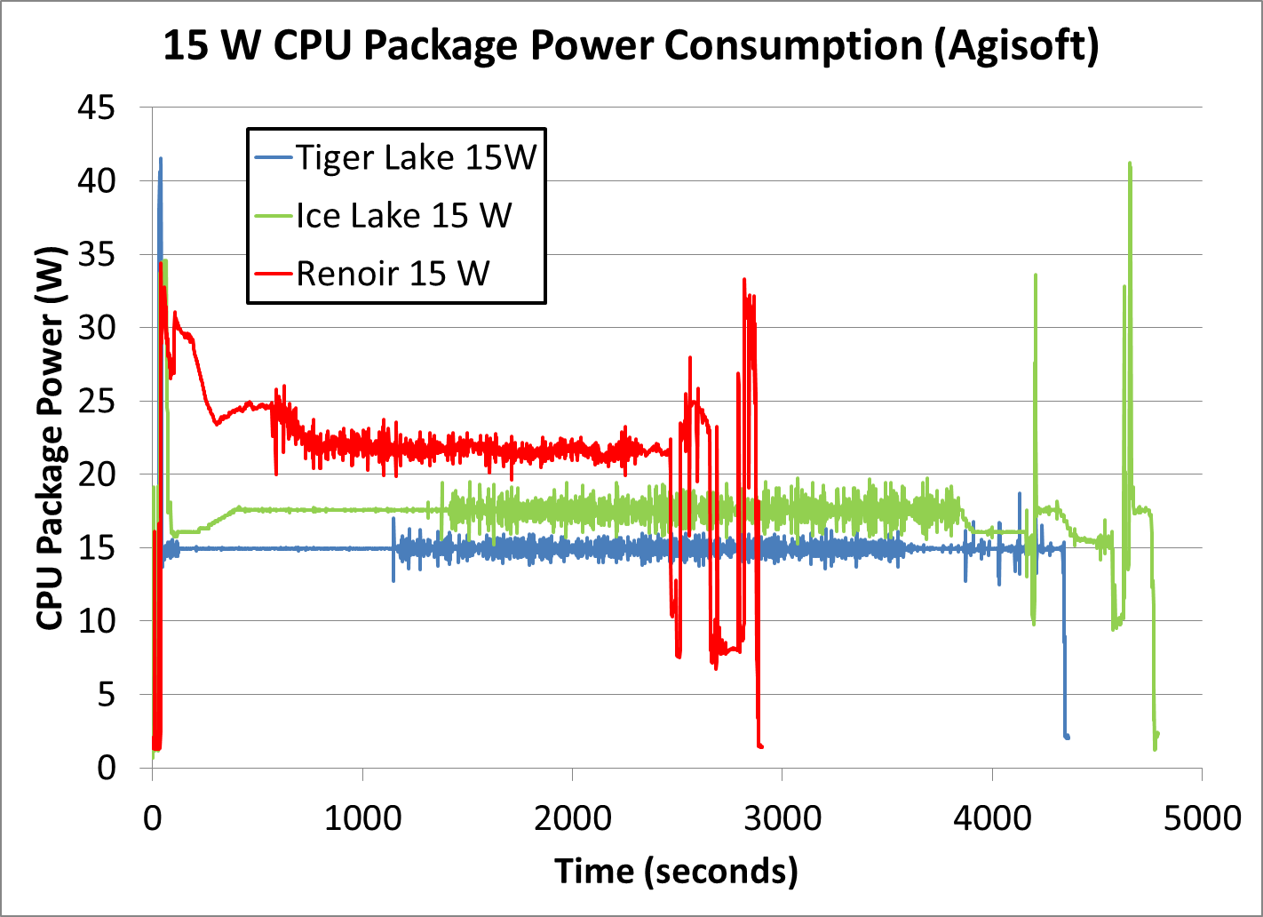
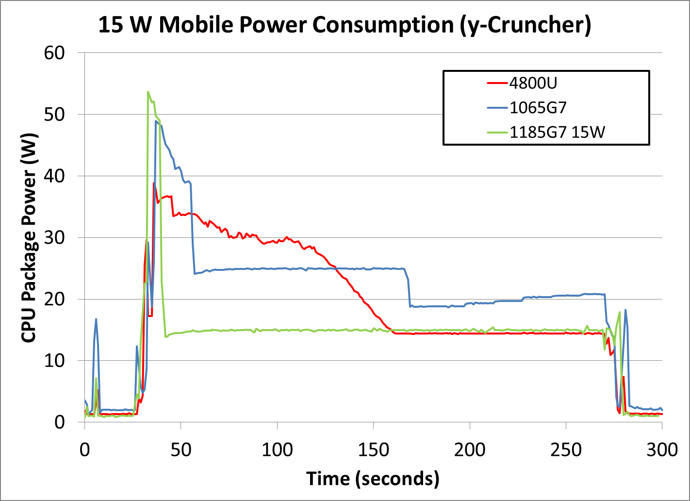
But the TDP is also configurable. It's one of the main differences between different model numbers with the same number of cores which are actually based on the same silicon. The difference between the 4800U and the 4900H is only the TDP and the resulting increase in clock speed. But the TDP on the 4900H goes up to 54W.
Whereas the TDP on the 4800U they tested there is configurable even within the same model, from 10-25W. And then we see it there using a sustained 20-25W, which is perfectly within spec depending on how the OEM configured it. And there is presumably a setting for "use up to max power as long as not thermally limited", which is apparently what they used, and then combined it with a 15W cooling solution. Which is what you see clearly in the first graph on the same page:
It uses more power until the thermal solution doesn't allow it to anymore.
In the second test it can sustain a higher power consumption, maybe because the test is using a different part of the chip which spreads the heat more evenly instead of creating a hot spot. But this is all down to how the OEM configured it, regardless of what they advertised. That CPU is rated for up to 25W and is only using 22. Obviously if the OEM configures it to use more, it will.
yes, but if the 7945HX3D is running at 112W (75W cTDP + AMD allows unlimited-duration boost at 50% above this) and the macbook is running at 50W cpu-only (70W TDP) then the macbook is actually substantially more efficient in this comparison.
That's why I said: you have to look at the actual power measurement and not just the box spec, because Apple generally undershoots the box-spec for cpu-only tasks, and AMD always exceeds it substantially due to boost. Obviously if you give the AMD processor twice the power it's going to be competitive, that's not even in question here. The claim was, more efficient than Apple - and you simply cannot assess that with the box TDPs, or even cTDPs, because x86 processors make a mockery of the entire concept of TDP nowadays.
(and it didn't use to be like that - 5820K and 6700K would boost to full turbo under an AVX2 all-core load within the rated TDP! The "boost power is not the same thing as TDP" didn't come around until Ryzen/Coffee Lake era - accompanied by ploppy like "electrical watts are not thermal watts" etc)
edit: notebookcheck has cinebench R15 at 36.7 pt/w for M3 Max and 33.2 pt/w for 7840HS, and 28 pt/w for Pro 7840HS (probably a higher-cTDP configuration). Obviously CB R15 is miserably old as a media benchmark, but perhaps ironically it might be old enough that it's actually flipped around to being more representative for non-avx workloads lol.
CB24 MT at 50% higher for M3 Max and CB R23 at 11% higher (shows the problem there with x86 processors on R23). Looking back at Anthony's review-aggregator thing... they're using the highest score for 7840HS I would assume (it's 1k points higher than median on notebookcheck) and also they're probably comparing box TDPs, which is where the inversion comes from here (from parity to a 10%-ish lead on efficiency). Because actual measurements of the M3 Max, from actual reviewers, have CB 2024 at around 51W all-core, and it almost doubles a 7840HS's score there.
And looking at it a little further even that nanoreview aggregator thing doesn't claim 7840HS is more efficient... they rate the M3 Max as being 16% more efficient. Seems that is a claim Anthony is imputing based on, as I said, box TDP...
edit: I’m also not even sure that nanoreview article has the right TDPs for either of them in the first place…
OT: I think it also shows the bad iGPU compared to Apples offerings, so too many x86 laptops have additional GPUs, which reduces battery life (we'll see what Strix brings)
Also both have 16 performance cores, but the Ryzen is faster in multicore. The Ryzen is one year later b/c due to node access/ costs. Doesn't look like "far behind".
There is nothing inherently inefficient about a discrete GPU. Discrete GPUs often have extremely good performance per watt. That's just not the same thing as having a low TDP. Performance per watt is higher when something is twice as power hungry but three times faster.
Not an electrical engineer, my GPU board has lots of additional chips and VRMs, and I do think those should take additional power. All of these are cooled which means they convert power into heat, so I would assume a discrete board draws more power than a SoC. But as I've said, not an electrical engineer (Just some electrical engineering exams at university).
In principle you can shut off anything when it's idle and get its power consumption arbitrarily close to zero.
Discrete GPUs obviously use more power because their use case is when the iGPU isn't fast enough. Hypothetically you can make a discrete GPU with the same performance as an iGPU and it would be no more power hungry. These have occasionally been available, basically monitor cards for CPUs without an iGPU etc. But the ones with a lot of fans and VRMs have them because they do indeed use a lot of power -- which isn't the same as having poor performance per watt, because they're also really fast.
Do you have benchmarks though? TDP is a poor metric for comparison because it varies significantly by manufacturer and doesn’t encapsulate the performance curve at all.
Sorry, I dropped a few words accidentally before submitting and it’s too late to edit it :-( my bad.
I meant to ask for benchmarks across the power spectrum (measured by actual pull not OEM TDP) and off charger. That’s where the x86 processors down clock heavily to keep power in check, and M series pulls ahead because it doesn’t follow suite.
The M series, even at launch, weren’t the king of outright perf, but they were for power to perf.
The M series at launch was already on TSMC 5nm when nothing else was yet.
The problem with asking for benchmarks that actually measure power draw is that somebody would have had to have done them, which hardly anybody does, and specifically on the few CPU models that were made on the same process. So if that's what you want to see, where are yours? Find a comparison that actually measures power draw between two CPUs with similar performance/TDP on the same process, like the M1 Ultra and the Ryzen 7945HX3D.
> That’s where the x86 processors down clock heavily to keep power in check, and M series pulls ahead because it doesn’t follow suite.
That's not really how either of them work. CPUs from any vendor will run at lower clocks under threaded workloads in order to meet their power budget. This is also why the high core count CPUs actually have the best performance per watt -- the cores are clocked lower which is more efficient but you still get the performance from having more of them. And then "race to sleep" etc.
Apple optimizes for IPC and power, that means wide architecture and large die area. The rest optimize for throughput and cost. That means small dies and higher power consumption.
AMD and Intel can do what Apple does and Apple can do what AMD and Intel do, but each company chooses the path they believe it makes more sense for them.
When first launched, the Apple CPUs did about 50% more work per clock cycle (i.e. more instructions executed simultaneously) than the best Intel and AMD CPUs, enabling a 3.2 GHz Apple CPU to have the same single-thread speed as a 4.8 GHz Intel or AMD CPU.
Because the power consumption grows at least quadratically with the clock frequency, having the same speed at a lower clock frequency provides better energy efficiency.
Meanwhile, the difference in IPC (instructions per clock cycle) between Apple and the others has been reduced, but Apple still has a healthy advantage.
The different microarchitecture explains the energy efficiency advantage for single-threaded tasks.
On the other hand, for multi-threaded tasks, the power consumption per chip area is limited by cooling and the energy required to do a quantity of useful work (which is done by switching a certain number of logic gates) is mainly determined by the parameters of the CMOS process used to make the CPU die (assuming that the CPU designers are not incompetent).
So for multi-threaded tasks the better energy efficiency of the Apple CPUs has been determined mostly by the fact that they have been the only company able to use the latest and greatest TSMC CMOS process.
Apple jumped onto the split-core train early on. High performance cores for being good in IPC and low performance cores for multi core workloads with overall low power usage.
Apple has the benefit of controlling the OS, so no scheduler problems.
Intel came later but seems to make good advances, if you look at e-Cores in Lunar Lake.
I predict AMD will go the same route (way bezond 5c), now that x86 also focuses on performance/watt and not peak performance (if you watch the announcements).
Apple jumped onto the split-core train early on, because it was the first having access to more advanced manufacturing processes.
CPUs with big and little cores were not useful for the old "14 nm" manufacturing processes used by Intel for Skylake and its derivatives, because in those processes the power consumption of a core and its speed could be varied in a very large range, e.g. for the extremes of the supply voltage, the clock frequency of a laptop CPU core could vary between 0.6 GHz and 4.5 GHz, corresponding to a variation of the power consumption per core of even 50 times.
Modern processes have more constrained ranges for the optimal operating parameters of the transistors, so it has become better to split the cores into several classes that are designed with different trade-offs between power consumption and performance, instead of attempting to use the same core both at very low and at very high power consumptions.
The decision to use 2 or more kinds of cores to cover the entire curve of performance vs. power consumption, when you can no longer cover it by varying the operating parameters of a single kind of core, is a no-brainer.
While for the CPUs with a small number of cores, like for smartphones, tablets and light laptops, the existence of multiple kinds of cores is needed for optimum energy efficiency, the CPUs for desktops or big laptops with a great number of medium-size cores, like Raptor Lake, have them for a different reason. The big Intel cores, in the quest for maximum single-thread performance, have poor performance per chip area. The medium-size cores have better performance per area, so in the same limited chip area you can put more cores, increasing the multi-threaded performance beyond what would be obtained by filling the same area with big cores.
Nevertheless, AMD has a better strategy than Intel, because their big cores with high single-thread performance and their "compact" cores with better performance per chip area are logically equivalent, avoiding the software incompatibility problems caused by Intel.
> the Lunar Lake SoC platform also includes up to 32 GB of LPDDR5X memory on the chip package itself. This is arranged as a pair of 64-bit memory chips, offering a total 128-bit memory interface. As with other vendors using on-package memory, this change means that users can't just upgrade DRAM at-will, and the memory configurations for Lunar Lake will ultimately be determined by what SKUs Intel opts to ship.
In other words, even though it's on-package, the width of the memory interface is the same as previous generations. They also exclude upgradability unnecessarily, because even with on-package memory you can still support adding memory through slots. For example, the Xeons with on-package HBM allow this.
This decision by Intel seems specifically designed to screw the customer by forcing them to buy a new CPU (or computer) in order to upgrade the memory, without even providing the countervailing benefit that Apple gets from doing it that way. (Note that Apple too unnecessarily prevents adding memory at the traditional level of performance. Cache hierarchies are a thing, if you're not trying to screw the customer.)
There is no way that you can get a 40% reduction in total CPU power consumption, much less system power consumption, just by lowering the voltage of the memory -- the entire contribution of the memory is a tiny fraction of the system's power budget.
Reducing power consumption by an imperceptibly small fraction of a fraction of a percent is just an excuse.
My thinking is that we may be seeing MSFT working to commoditize CPUs and in the process end up strengthening their position while weakening ARM, AMD, and Intel's positions.
In the past MSFT was always wedded to x86 but now with other ISAs coming, that presumably Windows 11 can be ported to...
No one bought it on those alternative ISAs, however. The Alphas and MIPS vendors had a port but what percentage of those systems ended up running a Unix? This time it is different since DOS and 16bit Windows is out of the picture.
This time you have multiple vendors/OEMs actually shipping e.g. Snapdragon-based Windows systems. Lenovo might make money selling such laptops, but over time MSFT will be the largest beneficiary of the "CPU wars".
There was Windows RT, which failed, but the current Windows on ARM platform has been a thing since 2017. The first few Win10 on ARM devices aren't upgradeable to Windows 11, but anything since the Snapdragon 850 in 2018 is fully supported by Windows 11: https://learn.microsoft.com/en-us/windows-hardware/design/mi...
I guess it could still fail, but to me it seems a bit weird to be predicting the failure of a 7 year-old platform just when it's starting to see a real uptick in momentum.
When it comes to porting Win11, does MSFT have something like Rosetta to ease the pain for applications during the transitional period?
Sure, plenty of windows users (business and personal computing) rely primarily on first-party apps, browsers, and big flagship apps (which could presumably leverage Microsoft partnerships to release on new architectures early enough that users wouldn’t notice much pain). But the long tail of widely used applications that aren’t big enough that I’d trust them to release ports by the time of an ARM (or whatever) hardware release is huge in Windows land—much larger than on MacOS.
Rather than MSFT it is just becoming a natural progression - we used to have a lot of various CPU makes in the past too at one point. With ARM now everybody can ship their processors.
Intel, AMD, Nvidia, Qualcomm + big tech giants like Apple are already producing them, MSFT is also planning to do that. I recall either Google or Facebook wanted too and so on.
Although memory bandwidth is still a limiting factor, I still hope those improvements at the integrated gpu ship over to their desktop counterpart. AMD seems to get at it already.
(Yes Yes, I know I know. But I am still dreaming to fit a system capable to play at least a few games into a mini itx case without needing to add a dgpu. One can dream, eh? :)
It’s sounding like AMDs high-end mobile processors will probably do what you want mid-to-late next year. Look up “Strix Halo” (not Strix Point, that’s this year).
They’re reportedly going for a 256 bit memory interface, and a way bigger GPU than what’s normal for integrated graphics.
I mean, AMD (together with Intel!) was already there, with their KabyLake-G lineup. Intel processor and AMD Vega (although it was Polaris Arch, I think) Graphics together along with 4 GB of HBM 2 graphics memory.
Or all those custom APUs, AMD is doing since quite some time, like way back in 2018 for that Chinese computer / game console thingy (Subor Z+). Or for the new wave of handheld game consoles. And last but not least for the Playstation / XBox.
That packaged onto a Mini-ITX mainboard along with 32 or 64 GB of RAM would be quite nice.
I meant in general like in for gaming uses, integrated gpus are limited by the memory bandwidth of the DDR memory bus compared to the high bandwidth memory on dgpus.
Buy something else? Meteor Lake supports up to 96GB, and I assume AMD has something that supports 64GB+ as well.
Lunar Lake is specifically targeted towards power efficient laptops, there are no desktop chips, or desktop-class mobile chips. Its being positioned for Macbook Air competitors, a device which maxes out at 24GB RAM.
It is an offering for low power segment with integrated graphics and an AI unit. I doubt intel is breaking into phones any time soon so I have no idea where this will be used.
The really big deal there is that this is an Intel processor built at TMSC.
Most things (other than highly optimized HPC) benefits a ton from hyper threading. Code that's unoptimized (e.g. everything web/interpreted languages like python/JS) spends all its time chasing pointers which means that your cores are doing a whole lot of nothing. Hyperthreading means that you can run twice as many applications per core which means that while one thread is waiting for data from RAM, the other thread can utilize the execution units. This also helps power consumption since if you can consolidate all the tasks onto fewer cores, you can put the other cores to sleep and save power.
Likely true in some cases but are these the bottlenecks on a laptop? I've never experienced HT on a multicore CPU being more than maybe a 40% increase in throughput and no real help on latency or efficiency. Implementing HT isn't free and doubling the number of active processes halves the per-process cache while doubling the concurrency in the memory controller (or more because less cache). Then there's the scheduler complexity... On the other hand there's the dual efficiency win of adding more E cores with shorter/simpler pipeline and lower clock speeds.
Back in the P4 days HT made desktop interactivity much smoother, these days with 8+ core laptops the win is less clear and at least some of the top design teams think it's not worth it.
As a software developer, by far the most imortant advantage of SMT is the reduction in compilation time for big software projects.
I have not encountered any other application that benefits so much from SMT as a compilation that uses all available threads.
On older CPUs, such as Skylake derivatives, a 25% compilation speed improvement from SMT was frequent. On newer CPUs, e.g. Zen 3 (presumably also on Zen 4, which has a very similar microarchitecture), the benefits of SMT are smaller (due to improved out-of-order execution), but a 20% compilation speed improvement is still frequent.
However, doing compilation on a device with Lunar Lake, a CPU with only 4+4 cores, would be a waste of time, so it clearly does not need SMT.
On the other hand, doing compilation on a bigger laptop, with an AMD Strix Point 12-core/24-thread CPU or with whatever Arrow Lake CPU will be launched by Intel to compete with it (presumably having much more smaller Skymont cores than Lunar Lake, to compensate for the lack of SMT) would certainly be useful.
When compiling an entire Linux distribution, there are a few outliers, all of which are derivatives of the Google Chrome code base, which may fail when less than 2 GB is available per build thread (e.g. for a 16C/32T CPU with make -j32, 64 GB of DRAM are required).
For most other software projects 1 GB per build thread is enough.
This isn’t really true. In JS, the JIT can optimize many routines to be much more CPU bound than “just pointer chasing” would have you believe. And of course in Python the bulk of your time should be spent in native code. Whether it actually is is a different question.
If a load is intrinsically pointer chasing (as it is the case for a lot of non-compute software), there isn't much an optimizer can do. That's true even for native code.
I've always thought of HyperThreading as marketing with no substance. I've seen applications run slower with HT turned on (admittedly a long time ago). Does this combination of running two threads that are "poorly" written (i.e. they can't make use of all the execution units) really exist? If you're multitasking applications you very rarely have multiple application simultaneously require a lot of CPU cycles (e.g. you might be switching from a spreadsheet to a browser but not doing heavy work on both simultaneously). If you are running some specific heavy computational workload then likely it's already optimized to fully utilize the cores it is getting and HT can actually get in the way of that.
>If you are running some specific heavy computational workload then likely it's already optimized to fully utilize the cores it is getting and HT can actually get in the way of that.
You can test that by running Cinebench with and without hyperthreading. In most of the cases hyperthreading does help.
A lot of rendering benefits from having SMT/HT disabled. Almost every film studio will do so.
Having accurate hardware thread counts matter in those scenarios because the renderers will basically peg each core completely , and the risk of having an SMT/HT context switch between them is detrimental. It was often up to a 30% speed decrease when HT was enabled for us in production scenes.
Similarly , many games run better without HT.
HT primarily benefits scenarios with many smaller jobs without latency sensitivity.
Today though, E-cores have largely replaced the need for HT. It’s much easier to send them to an E core and have them done without the extra overhead of HT scheduling and support.
Sure, they can just disable the feature. I’m just responding to the person who is pointing at Cinebench as a reason to enable it, but in real world use cases it actually ends up being a detriment.
I meant that most people can leave it on. And if the software creator knows its not good for their software they can just not use HT cores, without disabling HT completely.
There are server workloads like maybe high concurrency web apps that might benefit. Back in the days of single core CPUs HT made desktops feel a lot better not just because of throughput but (my speculation) because it reduced typical scheduling latency. Antivirus or whatever else was happening in the background was less likely to cause UI jank.
According to comments from Intel, the additional hardware that has to be added for SMT on a P core isnt much smaller than an entire E core. So, they decided it is better to just rely on the E cores for additional multithreaded performance.
I dont think apple silicon supports SMT? Isn't that enough evidence to show at least for mobile parts 4P4E at least has a chance to be interesting? Also some of the graphs appear to show the new Skymont uarch has high perf/w than raptor cove (the previous P core) which is rather impressive in my opinion.
Nothing. When you want more throughput, pick a setup with more cores. HT was good (not that good but still good) when the goal was performance per die area, but now we live in the area of performance per watt. Doubly so when looking at laptops, but also in all other areas except perhaps gaming PCs (but even there, throughput at high wattage will eventually lead to throttling).
> I'm talking about these new things with ram integrated into the SoC...
But you were already told that this limit is just for this entry-level series of chips.
You asked what other series of Intel chips supported more memory, and the answer is all of them. If your question was supposed to not be about other chips, then your question makes no sense to me. And if that's the case then why did you bring up Xeons and your previous box?
I last bought an x86 box like 3 years ago, and it was AMD. Iirc back then consumer Intel CPUs supported less maximum ram than amd, hence the Xeon reference.
At the moment I have no idea what either Intel or AMD sells exactly. But I expect the worst.
I'm so tired of soldered components. The performance and power benefits are simply not good enough to justify producing millions of landfill-destined devices and high costs for consumers.
I don't think soldered components would have been a big deal were the amounts enough. 32gb soldered on say 7 years ago would last you a long time. If they're gonna solder, they need to stop skimping.
One other major problem with soldering is only the most common SKUs are in stock, at least if you're in a smaller market. I mean, I hope the US is different, not sure if that's true.
If you want to future proof and max out the ram you have to wait. And if you need an emergency hardware replacement, you're screwed.
I like to pretend I know a thing about CPU design, but I have to admit, I have no idea what's going on here.