Apples M1 only worked because everything is in one chip. Very different from the goals of framework. There aren't any vendors offering M1 competitors either.
Because there’s no evidence for the claim, and the evidence is mostly “Apple has created a huge and complex chip”?
And what does “Everything is in one chip” even mean? Because the memory certainly isn’t, it’s soldered on the package but it’s not part of the package, it just doesn’t take additional room on the main board. And there are a bunch of other chips on the mainboard
Finally, it’s pretty much just following mobile / phone chip SoC design, so any other manufacturer could do the same, if they wanted to create a giant and expensive SOC.
And I want to be really clear on the “giant and expensive” part: the M1 family is the sort of scale you usually see on giant workstation or server chips, the M1 Pro has 33.7 billion transistors, that’s more than a Threadripper 5995WX, a $6500 64 cores CPU. The M1 is just short of the 5950X’s transistor count (16 billions to 19.2), the M2 is above (~20).
> And what does “Everything is in one chip” even mean?
I guess he's mainly thinking of GPU, which isn't unique. But there's not that many SoCs with that amount of power in one SoC. So it's close to competing with alternatives with discrete GPUs, which does increase power consumption.
I believe it has integrated Flash controller too, which is very unique for a laptop/desktop chip, no?
> Because the memory certainly isn’t, it’s soldered on the package but it’s not part of the package, it just doesn’t take additional room on the main board. And there are a bunch of other chips on the mainboard
It's on the package so it can be as close to the SoC as possible. That decreases the capacitance of the traces, which decreases power consumption.
It's not stacked on top of the SoC, which might have been even better (but harder to cool), but it's close.
> Finally, it’s pretty much just following mobile / phone chip SoC design, so any other manufacturer could do the same, if they wanted to create a giant and expensive SOC.
Uh, yeah, anyone could copy the M1 for a laptop/desktop product. But they haven't exactly done that yet have they? That's kind of the point?
> the M1 family is the sort of scale you usually see on giant workstation or server chips
Yeah, which again, almost never packs the kind of functionality Apple does into the M1.
With that many transistors, on such an advanced process, you're going to have a lot of leakage currents, so Apple must have put an impressive amount of work into power management.
I mean, it's not just about being an SoC with lots of things packed within the chip or extremely close to the cheap (memory). No. It's apparent that they've focused on across the entire design process. Even the choice of ARM factors into that (fewer transistors needed for instruction decoding). But I wouldn't say the original comment is completely wrong.
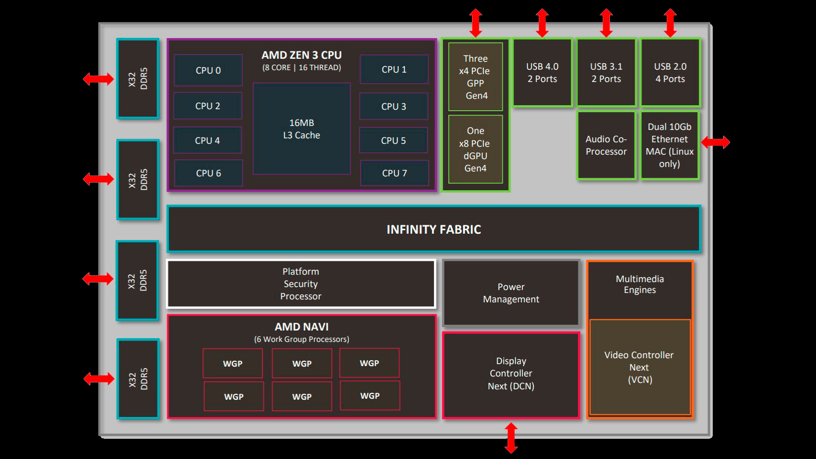
Even on the desktop processors, there are onboard lanes dedicated to the NVMe itself, and the entire processor (including NVMe) is capable of booting without a supporting chipset at all - the "X300 chipset" is actually not a chipset at all, it is just using the SOC itself without an external chipset, and you do not lose NVMe functionality.
Not sure if you are using some really weird meaning of "NVMe controller" that doesn't match what anyone else means?
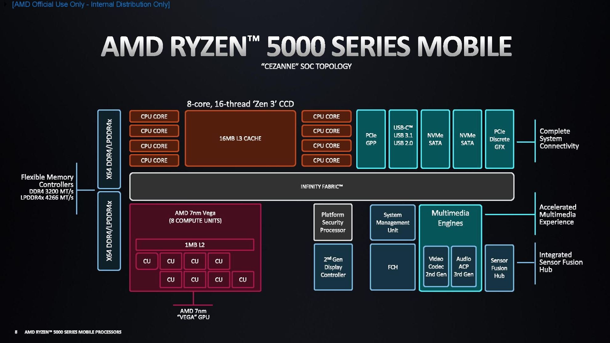
I meant the controller that manages the NAND cells, I assumed it would be called NVMe controller. Essentially the IC that the "NVMe controller" in your image talks to.
That would normally be called a "flash controller" and yeah, of course that lives on the SSD.
(unless it doesn't - eMMC doesn't normally have a flash controller and you just do direct writes to the flash cells... as do some IOFusion PCIe cards that are just flash directly attached to PCIe with no controller. Sometimes that functionality is just software-based. Flash cards (eg microSD) usually also do not have a flash controller directly either.)
Anyway, it's true though that Apple does push the flash controller functionality into the SOC while AMD does not, Apple implements their SSD in a non-standard fashion, that's why it's not compatible with off-the-shelf drives. The flash is just flash on a board, I don't even think it's NVMe compatible at all either.
So if you want to be maximally pedantic... neither does Apple implement onboard NVMe controllers, just flash controllers ;)
FYI, all current flash card formats have the equivalent of an SSD controller, implementing a Flash Translation Layer. Exposing raw NAND was somewhat viable in the very early days when everything was using large SLC memory cells (see SmartMedia and xD-Picture Card), but no current format could remain usable for long without wear leveling. If you can use standard filesystems and access the drive or card from multiple operating systems, then it must be providing its own FTL rather than relying on the host software for wear leveling.
The above also applies to eMMC and UFS storage as found in devices like smartphones.
AMD processors provide PCIe lanes, some of which are intended for use with NVMe SSDs but nothing on the chip actually implements or understands NVMe and the lanes used for the SSD in a typical system design are still fully generic PCIe lanes.
> nothing on the chip actually implements or understands NVMe
pretty sure that's false as well... can an X300 system boot a NVMe drive? I'd assume yes. It does that with a UEFI which lives... where? Oh right, on the chip.
Most NVMe SSDs don't provide legacy option roms anymore either.
> It does that with a UEFI which lives... where? Oh right, on the chip.
No, UEFI is firmware stored on a flash chip on the motherboard, usually connected to the CPU through the LPC bus. CPUs do not have any nonvolatile storage onboard (unless you count eFuses).