Yeah overall feature size isn't 1 to 1 with the "process" anymore, hasn't been there for a long time.
All of them use various sub-wavelength techniques like using multiple stencils and masks to create aperture / fresnel lense like effects etc.
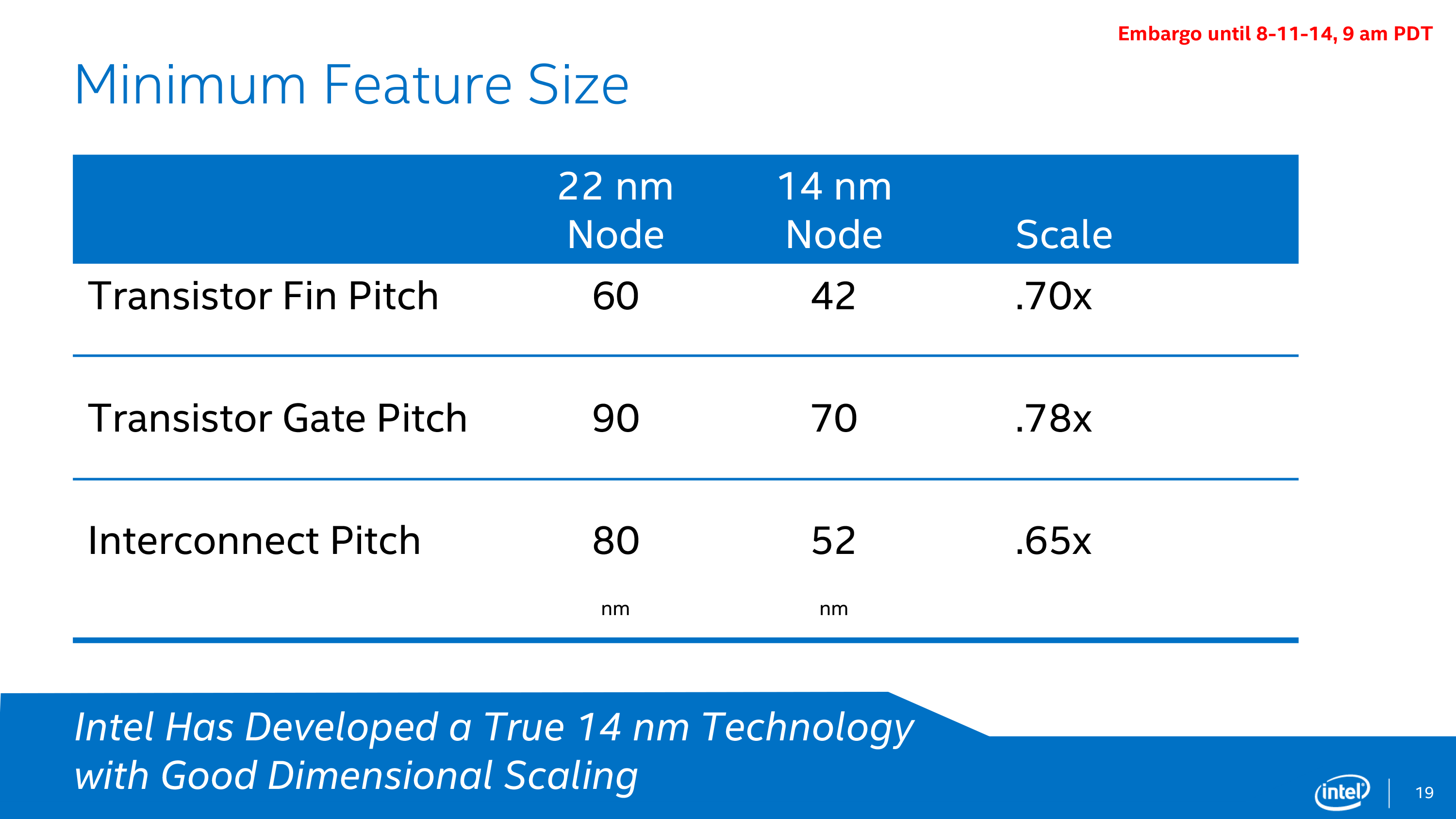
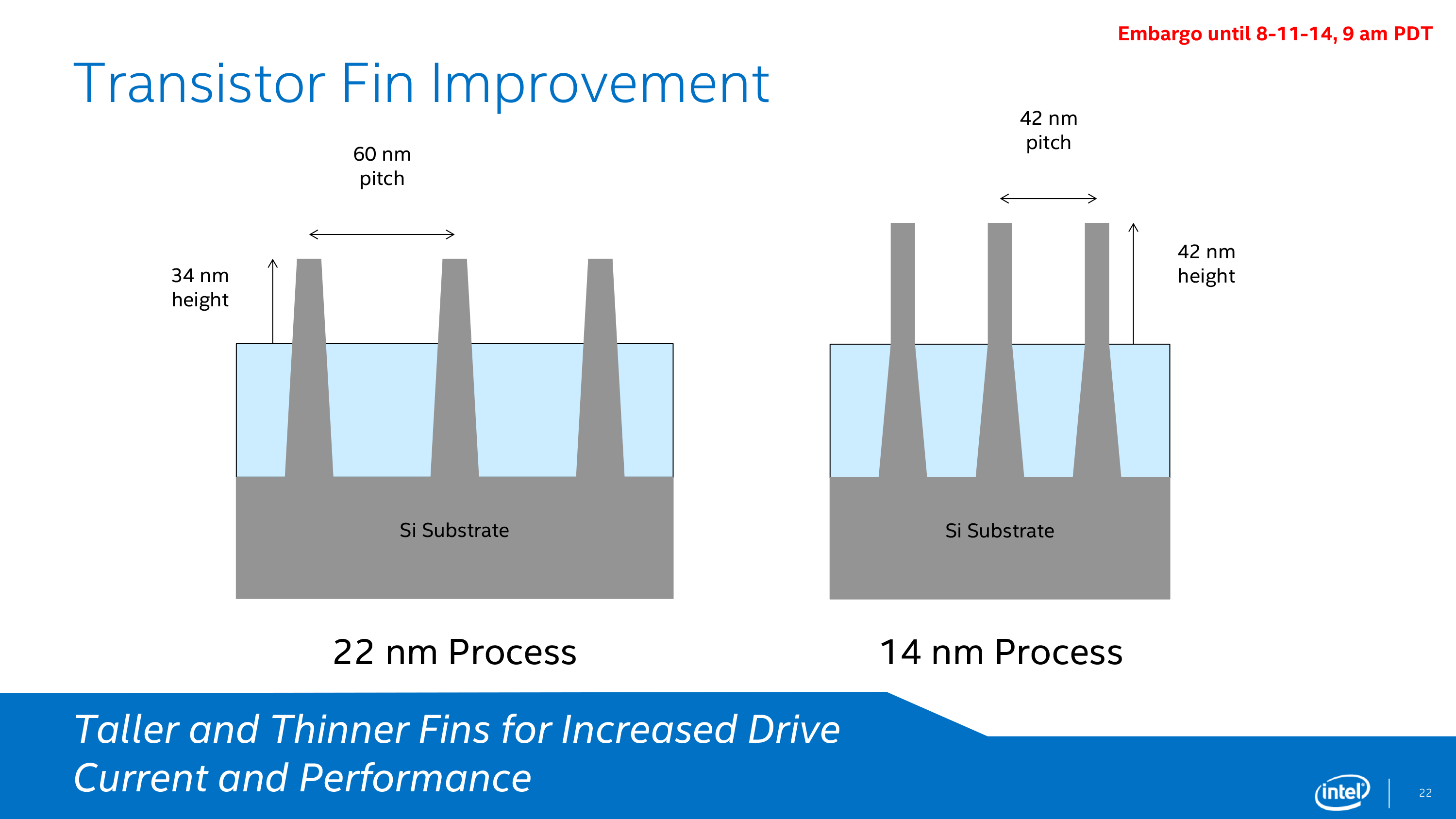
Pretty much since you have multiple measurements for "feature size" like fin, gate, interconnect pitch etc. companies are just naming their process roadmap to show "progress".
I don't think even Intel's 14nm process actually has a 14nm "feature size" and if it does I don't know what measurement they are basing it on.