Chris Tarnovsky is amazing, a true prodigy. Unfortunately, he gets bad advice on how to present his work. TPMs are what the media latched onto but are almost irrelevant to his advances.
What Chris presented is a full break of the Infineon SLE66PE secure microcontroller, used in smart cards for applications such as pay TV. This is one of the best of the current generation of smart cards. All of them have a layer of metal mesh that allows the chip to detect probing attempts. This processor also has optical sensors below that mesh (defense in depth?) It has many other countermeasures to prevent invasive attacks.
Chris's work in this area is astounding. He's now using a FIB whereas before he was just using microscopes and chemicals. This allows him to burn holes or deposit metal in the low tens of nanometers range. Combined with his old skills, this makes for a formiddable platform for defeating chip security measures.
His work on this chip is not easy, nor is it easily replicated. However, once someone with the resources and skills performs this kind of attack, it can enable much cheaper attacks later. For example, using this method to dump the ROM and then finding a software flaw in it would allow for attacks using ordinary PCs, no more physical manipulation needed. Or, you can build a jig ("drill here") that lets it be replicated by less skilled people using microprobing needles and ordinary microscopes. This reduces the cost of subsequent attacks.
TPMs have a poor security model to begin with. The exposed wires on the LPC bus (4 x 16 mhz) can be used to MITM it. The entire design is not meant to resist even board-level attacks, let alone invasive chip work. Claiming his talk is about TPMs is like saying cryptanalysis of SHA-1 is about breaking Django authentication. Sure it does, but there are much more important affected applications.
I actually think this validates the SLE66PE design. The fact that it required this much work gives me much more confidence about using it. Hopefully Infineon uses the information from Chris's talk to improve the next generations.
EDIT: To those who downvote me, that's your privilege, and I have no complaints. To explain, I do it to try to prevent identical or nearly identical comments being spread over several submissions. As a programmer/hacker, I prefer the principle of DRY - don't repeat yourself - and having comments on the same item in several places just leads to unnecessary duplication and just seems messy.
I wish there were better duplicate detection, or a way of merging the comments from multiple items, but there isn't. This is one way I try to add value to HN - to save time by highlighting these duplications.
If you genuinely think this is damaging behavior then I'd be interested to hear why.
Deep inside millions of computers is a digital Fort Knox, a special chip with the locks to highly guarded secrets, including classified government reports and confidential business plans.
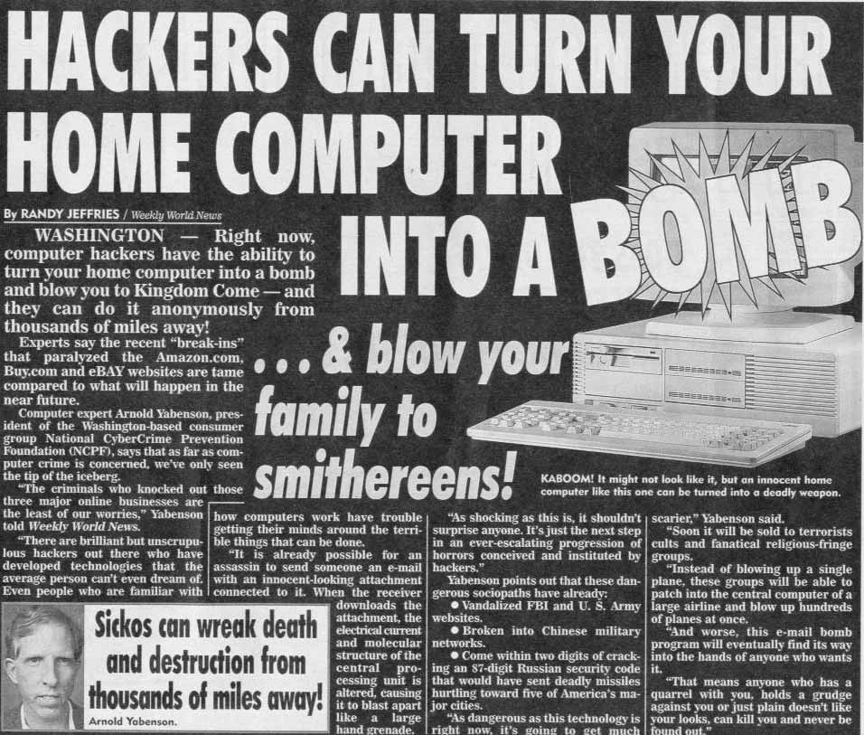
How can someone write this without chuckling? A "digital Fort Knox"? Seriously, this style is getting far too popular recently. Reminds me of "Hackers Can Blow Your Family to Smithereens!" http://1.bp.blogspot.com/_7YnlMQU1TNI/Sw6SxbYzoLI/AAAAAAAADL...
What Chris presented is a full break of the Infineon SLE66PE secure microcontroller, used in smart cards for applications such as pay TV. This is one of the best of the current generation of smart cards. All of them have a layer of metal mesh that allows the chip to detect probing attempts. This processor also has optical sensors below that mesh (defense in depth?) It has many other countermeasures to prevent invasive attacks.
Chris's work in this area is astounding. He's now using a FIB whereas before he was just using microscopes and chemicals. This allows him to burn holes or deposit metal in the low tens of nanometers range. Combined with his old skills, this makes for a formiddable platform for defeating chip security measures.
His work on this chip is not easy, nor is it easily replicated. However, once someone with the resources and skills performs this kind of attack, it can enable much cheaper attacks later. For example, using this method to dump the ROM and then finding a software flaw in it would allow for attacks using ordinary PCs, no more physical manipulation needed. Or, you can build a jig ("drill here") that lets it be replicated by less skilled people using microprobing needles and ordinary microscopes. This reduces the cost of subsequent attacks.
TPMs have a poor security model to begin with. The exposed wires on the LPC bus (4 x 16 mhz) can be used to MITM it. The entire design is not meant to resist even board-level attacks, let alone invasive chip work. Claiming his talk is about TPMs is like saying cryptanalysis of SHA-1 is about breaking Django authentication. Sure it does, but there are much more important affected applications.
I actually think this validates the SLE66PE design. The fact that it required this much work gives me much more confidence about using it. Hopefully Infineon uses the information from Chris's talk to improve the next generations.