NVIDIA are really keen you understand their hardware, to the extent they will give you insanely detailed tutorials on things like avoiding shared memory bank conflicts. It's rare to find so much detail from CPU vendors in my experience. Perhaps because CPUs, with their out of order execution and branch prediction, are just much much harder to predict and understand than the comparatively simple in order GPU cores.
At least for x86, there's an incredible wealth of architectural details out there, both from the vendors themselves and from people who have worked tirelessly to characterize them.
Along the lines of another comment on this post, part of the problem is the GPU compute model is a lot more abstract that what is presented for the CPU.
That abstraction is really helpful for being able to simply write parallel code. But it also hides the tremendous differences in performance possible...
Don't GPUs also have out of order execution and instruction level parallelism?
I think the reason why Nvidia publishes these resources is because the GPUs are worth nothing if people can't get a reasonable fraction of the advertisable FLOPs with reasonable effort. CUDA wouldn't have taken off, if it were harder than it absolutely needs to be.
> Don't GPUs also have out of order execution and instruction level parallelism?
Not any contemporary mainstream GPU I am aware of. Sure, the way these GPUs are marketed does sound like they have superscalar execution, but if you dig a bit deeper this is either about interleaving execution of many programs (similar to SMT) or a SIMD-within-SIMD. Two examples:
1. Nvidia claims they have simultaneous execution of FP and INT operations. What this actually means is that they can schedule an FP and and INT operation simultaneously, but they have to come from different programs. What this actually actually means is that they only schedule one instruction per clock but it takes two clocks to actually issue, so it kind of looks like issuing two instructions per clock if you squint hard enough. The trick is that their ALUs are 16-wide, but they pretend that they are 32-wide. I hope this makes sense.
2. AMD claims they have superscalar execution, but what they really have is a packed instruction that can do two operations using a limited selection of arguments. Which is why RDNA3 performance improvements even on compute-dense code are much more modest. Since these packed instructions have limitations, the compiler is not always able to emit them.
My understanding was that GPU instruction level parallelism is quite limited compared to CPUs (since multiple "threads" are running on each hardware core) and I wasn't aware that GPUs had any meaningful OOO execution.
This is arguable depending on your definition of ILP. CPUs try to extract parallelism from a single instruction stream in order to execute many instructions from the same stream in parallel. This is very costly in silicon area per instruction executed. GPUs don't need to do this because the programs run on them are "embarrassingly parallel" - they have lots of available parallelism and explicitly tell the GPU where it is. So GPUs execute many more instructions in parallel than CPUs, but they don't usually do any work to try and find implicit parallelism
Don't now if NVIDIA is keen to understand their hardware, but they are obviously very interested in users understanding their hardware. I originally started i86 assembler and stopped after the i860, which as far as I remember was the first Intel processor with branch prediction. It's a nightmare for control freaks, especially on CISC processors with variable clock cycles.
GPU programming with CUDA and PTX feels like programming on a single core CPU without tasks and threads with deterministic behavior but in a multidimensional space. And every hour spent avoiding an 'if' pays off in terms of synchronization and therefore speed.
The main problem with GPU architectures is that the manufacturers hide their details from us. Hell, they don't even document the instruction sets! At least NVIDIA doesn't. And they often don't tell us what the hardware actually _does_, and rather offer a mental model of how we can think about it.
Specifically, those structural diagrams of functional-units within SM's you see in the blog post? That comes from NVIDIA. And they explicitly state that they do _not_ guarantee that this is what the hardware is actually like. The hardware works "as-if" it were made up of this kind of units. And even more specifically - it's not clear whether there even is such a thing as a "tensor core", or whether it's just some hack for doing lower-precision FP math somewhat faster.
-----
Anyway, if the architectures weren't mostly _hidden_, we would make them far less mysterious within a rather short period of time.
> GPU instructions sets change every year/generation.
1. It's every two-to-three years.
2. It's not like they change into something completely different.
3. PTX is not a hardware instruction set, it's just an LLVM IR variant
4. I don't need to only target an instruction set directly, but it does help to know what instructions the hardware actually executes. And this is just like for CPUs (ok, not just like, because CPUs have u-ops, and I don't know that GPUs have those).
You can view it, but there's no documentation for it, nor a listing of all instructions. You need to guess what the instructions actually do. Sometimes it's not so difficult, like IADD3; but sometimes it's not at all trivial.
though there is no guarantee this is exhaustive, no opcodes either (though you could reverse engineer it using cuobjdump -sass and a hex editing like I've been doing). I'm pretty sure some of the instructions in the list are deprecated as well (95% percent sure that PMTRIG does nothing >Volta)
...But literally the exact same is the case for CPUs and yet we do have public and constant instruction set for decades now?
Altough ofcourse CPU's instruction are also just a frontend api that behind the scenes is implemented using microcode, which probably is much less stable.
But the point is, if we could move one level 'closer' on gpus, just like we have it on cpus, it would stop the big buisness gate-keeping that exsists when it comes to current day GPU apis/libraries
That's not true, you can run a 30 years old binary on modern CPUs. The machine code you feed to the CPU didn't change much.
That's not true for GPUs, the machine code changes very frequently. You feed your "binary" (PTX, ...) to the driver, and the driver compiles it to the actual machine code of your actual GPU.
But that's not inherent due to gpus completely revolutionizing their aproach every generation, is it?
The main difference is that with cpu, the translation unit is hidden inside the cpu itself.
With gpus, the translation is moved from the device to the driver.
Old openGL code also will run in card that is newer then code itself.
The only difference is that with the cpus, it's open standard what is the instruction set, while on gpus, instruction sets are defined by third parties (DX12,Vulkan,OpenGL) while it falls to nvidia to implement them.
OpenGL code is actually running on the CPU. From this CPU running code you can send shaders to the driver, in source code form or bytecode form, and the driver does the final compilation to GPU machine code.
Pedantry.
Yes you are running your code on the cpu, but you are using opengl defined api to do so.
Having a text generation and parsing, or having a function calls passed to/from drivers- those a simply implementation details
Modern CPUs being able to run 30 year old binaries as-is is pretty different than a GPU requiring a driver to compile byte code into machine code at runtime.
You seem like you're being purposefully obtuse about this, so I'm going to disengage after this. But, generally speaking, a programming language which compiles to machine code which is executed directly by the CPU is widely considered to have a significantly different architecture than one which is compiled to byte code to be executed by a virtual machine. This architectural choice has many downstream ramifications. And the difference in execution model between CPUs and GPUs is similar in nature and comes with similar ramifications. Such as, for example, operating system support for GPUs.
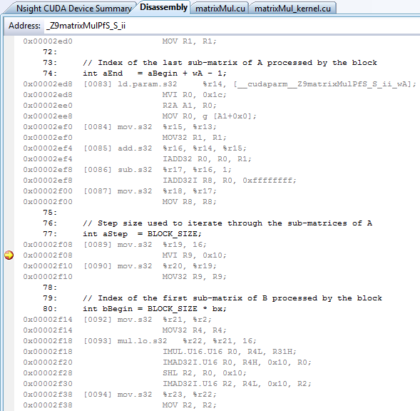
PTX is more or less the same as x86. What's even better is that unlike x86, Nvidia allows you to see and step through the SASS instructions which PTX compiles into. Although SASS is not documented, seeing it alongside the PTX makes it possible to infer the meaning. In contrast to this you can't see the micro-ops running on x86 cpus (although people have inferred quite a lot about them).
Just to be fair: as also stated at the beginning of the post, CPUs are far more complex nowadays than they represent themselves to the outside.
They don't work like a von-Neumann machine, they act like one. Granted, we know a lot more about the inner workings of modern CPUs thn GPUs, but a lot of real-life work still assumes that the CPU works "as-if" it was a computer from the 70s, just really, really fast.
Relying on the compiler to compensate for an unwieldy instruction set architecture is something that was tried explicitly with the Intel Itanium and failed hard.
\rant
I feel that generally people often have a notion of the "compiler is unbeatable at optimizing", which is completely false: You can always start from compiler output when optimizing and you often have easy options that are inaccessible for the compiler because of language semantics/calling conventions etc. (=> but hand optimizing at instruction level is time consuming, time is expensive, and what the compiler does is basically free ;).
Indeed, Nvidia has been awful about sharing documentation. The best docs I know of out Nvidia, are actually provided by Nintendo. AMD on the otherhand, while is far from perfect, does try to provide documentation.
Of course this doesn't apply to Nvidia, but MI-300 seems to be pretty viable for machine learning, so if you want things to change across the industry, more people need to put their money where their mouths are.
4 hours after posting, this is currently the second comment.
The first comment assures me "NVIDIA are really keen you understand their hardware, to the extent they will give you insanely detailed tutorials on things like avoiding shared memory bank conflicts."
I'd say NVIDIA is somewhat keen on you being able to utilize their hardware. So, they gave you some tutorials (absolutely not insanely detailed), documentation about the API, and a bunch of programming advice and recommendations. They also provide you with a mental model you could use to think about the GPU's work. But - that is all not the same as telling you what actually happens. They don't even publish instruction latency formulae, for example.
It's really great to see these kind of articles! Of course, this is just scratching the surface. I think the most challenging bit about understanding GPUs is breaking through the marketing claims and trying to understand what is really going on in the background. How are the instructions scheduled, how does the execution actually look like and so on. And this is where information can be very difficult to come by. Nvidia documents the "front-end" of their GPUs very well, but the details are often shrouded in mystery. It's easier with AMD, since they publish the ISA, but it can be still difficult to map their marketing claims (like 2x compute on RDNA3) to the actual hardware reality. Interestingly enough, we know quite a lot about Apple GPUs, since their compute architecture is very streamlined compared to other vendors.
Well this seems awfully surface level. This blogpost is essentially just dropping diagrams from AMDs and NVIDIAs documentation and reading the labels on them, with multiple mistakes that tell me that this person hasn't probably hasn't done GPGPU programming (what kind of instruction is "reciprocal"? it's the reciprocal sqrt)
Go read NVIDIAs developer docs and AMDs training material for Frontier for some actually useful introductory material.
For a deeper dive, Jia et al.'s "Dissecting the NVIDIA Volta GPU Architecure via Microbenchmarking" is your goto for NVIDIA material, along with NVIDIAs own documentation. For AMD, you should probably read the CDNA 2 ISA docs
Hi, Author here. Thanks for the feedback. I'm happy to correct any mistakes.
Sorry you don't think this is useful. However, as the post clearly points out it's not intended to make you a GPGPU programmer. That really isn't possible in a single blog post. Rather, it tries to give a general overview of how the GP part of GPUs works for the general reader, and to try to relate terminology used by AMD and Nvidia. I'm not aware of another source that tries to do this succinctly.
The end of the post gives lots of links for further reading for readers who want more.
And FWIW I have done quite a bit of GPGPU programming.
Thanks for responding, and sorry for the snide remark, I see a lot of blogspam on this topic and my bullshit detectors are sensitive.
My main gripe is that the blog post does not seem to explain any of the terms it's inteoducing. The text keeps promising to explain concepts that aren't brought up again, and the main differences between AMD and NVIDIA are not discussed (shared memory, warpsize). I did appreciate the history in the introduction, that part was well-written.
If you want to explain the GP part of GPGPUs, I would suggest starting with the threadgrid and moving onto threadblock register footprints and occupancy, it's been a successful recipe for me when I've been teaching, and it keeps the mental load low.
I wonder if at some point G(raphics)PUs and G(^HMachine-Learning)PUs will diverge to the point that we can start calling them different things. I don't particularly buy into the idea that 3D rendering is just an application of a bunch of compute units with a rasterizer at the end. There's certainly some alpha in graphics-dedicated hardware. Hey! Maybe we can call them "video cards" again!
AMD diverged RDNA (graphics) and CDNA (HPC/AI) already. Nvidia removed the graphics-specific hardware from Hopper although it appears to be a small fraction of the chip.
Hardware rasterizers are likely to disappear before long. We still use them because they are energy and area-efficient when working with large triangles. But already achieving high primitive count is difficult with hardware rasterizers, which is why some modern rendering approaches rasterize using computer shaders (e.g. UE3 Nanite). And of course, there is ray tracing which will replace the rasterization pipelines within the next decade or so.
As to ML, it absolutely needs different hardware than your traditional GPUs. The reason we associate the two is because GPUs are parallel processors and thus naturally suit the task. But as we move forward things like in-memory processing will become much more important. High-performance, energy efficient matrix multiplication also requires very different hardware layouts than your standard wide GPU SIMDs.
That’s the dream of HW GPU designers everywhere. I’ve got a bunch of dead Cell and Larrabee chips laying around upstairs that’d like to disagree, though. Coverage rasterization is just one tiny piece of the GPU story; the really hard parts (software-wise) are things like varying interpolation, primitive synthesis (and varying synthesis), change-of-basis, and specific sampling and blending modes. It turns out that once you add in the HW to make “a few edge cases” faster, you end up with all of the HW you need for a complete GPU.
Sure, there are things that will always benefit from some ASIC magic (like, I don't see texturing going away any time soon). And we even get new specialized hardware, such as hardware RT. But advances in both performance and rendering approaches make some of the old fixed-function unnecessary. For example, Apple already dropped most fixed function related to blending and MS — since they serialize the fragments before shading they don't get any race conditions. And from what I understand they don't have any interpolation hardware either, it's all done in the shader. Of course, they pay for all this convenience with additional fixed-function complexity of the TBDR binner, but I think this illustrates how an algorithmic change can make certain things unnecessary.
Tomorrow's real-time rendering is all about RT, point clouds, microprimitives, and all that interesting stuff, the fixed function rasterizer simply won't be as useful anymore.
I think the terms GPUs (for "regular pipeline" work - direct, opengl) and GP-GPU (for "custom pipeline" work - cuda, custom built) were used when I was working in the area some 15y ago.
Apple has three hardware units for machine learning (if you disregard the regular CPU FP hardware): the neural engine (for energy efficient inference for some types of models), the AMX unit (for low-latency matmul and long vector), and the GPU (which does contain some hardware for making matmul more efficient). Apple is a bit of a unique case since all processors share the same memory hierarchy, so they can afford to keep things separately. But I wouldn’t say that Apple has anything comparable to Nvidia’s Tensor Cores: AMX probably comes closest but it’s integrated with the CPU L2 and the total throughout is much lower. Unless you want FP64, that’s is very good compared to mainstream Tensor Cores.
All this stuff about warps and streaming multi-processors — is this still the best mental model for targeting modern GPUs with ML workloads? It seems cleaner to think in terms of GEMM, kernels, etc.
Without considering how memory is accessed (coalescing all accesses in a warp), your memory accesses will be up to the warp size slower (32x for NVIDIA). So basically, you can't write an even decently efficient kernel without considering this. And if you don't consider your available shared memory, that number will be much larger.
And these aren't advanced concepts, it's just the fundamental programming model for GPUs. It's on the level of "Access memory in predictable patterns, ideally sequentially" for CPUs. Everyone knows now that CPUs like arrays and sequential access. And GPUs like interleaved acccess, ideally in sizes no larger than your shared memory.
It is. A kernel is executed by a set of warps (or waves, AMD), the warps/waves define the SIMD-group that execute an instruction. Memory accesses that feed these SIMD instructions are coalesced into one operation, and therefore the optimal memory layout requires thinking in terms of warps.
Kernels are executed at some blocksize, and each block is executed by a SM. The SM partitions each have a limited set of resources, and therefore the number of warps (or waves, AMD) that execute simultaneously should be tuned according to the resources available (registers, shared memory, etc.).
The keyword to search for here is occupancy, and related topics include register pressure/spilling, shared memory and L1 cache-size.