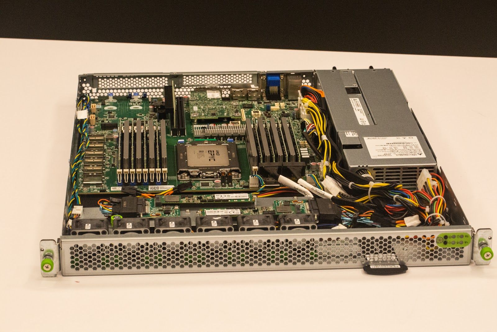
"Notably, for the first time, Intel is not inside. We are not using their hardware for any major server components such as the CPU, board, memory, storage, network interface card (or any type of accelerator)."
> This time, AMD is inside. We were particularly impressed by the 2nd Gen AMD EPYC processors because they proved to be far more efficient for our customers’ workloads. Since the pendulum of technology leadership swings back and forth between providers, we wouldn’t be surprised if that changes over time. However, we were happy to adapt quickly to the components that made the most sense for us.
> We selected the AMD EPYC 7642 processor in a single-socket configuration for Gen X. This CPU has 48-cores (96 threads), a base clock speed of 2.4 GHz, and an L3 cache of 256 MB. While the rated power (225W) may seem high, it is lower than the combined TDP in our Gen 9 servers and we preferred the performance of this CPU over lower power variants. Despite AMD offering a higher core count option with 64-cores, the performance gains for our software stack and usage weren’t compelling enough.
I find this a bit puzzling for density reasons. I can definitely appreciate the clock speed benefits. One 64-core part (AMD EPYC 7742) has the same TDP of 225W, so power should be in the same ballpark. There's also lower clocked 64-core SKUs with 200W TDP. I can't imagine price would be major factor for a company of Cloudflare's size, but it's definitely true that the 48-core part is much cheaper. There's also the 7H12 with a higher base clock than the 48-core part, but its TDP is 280W.
All of these EPYC chips have the same monstrous 256MB of L3, so maybe part of Cloudflare's workloads maxes out the cache before being able to feed all 64 cores, but that's a bit wishywashy. Maybe since they also all have the same PCIe lane capacity 48 cores is the sweet spot.
At least in my experience, for highly optimized code (which I imagine their's is), above certain core densities you run out of memory bandwidth, PCIe lanes, etc before you run out of cores unless your workload is particularly compute intensive. Power consumption also needs to be modeled into the hardware cost, so higher TDP does matter. It is a cost optimization problem, and those 64-core parts may offer little marginal gains for the added cost if bottlenecks are elsewhere in the system.
My experience buying CPUs for data intensive servers has typically been that maximizing the performance-density-cost curve often recommends a mid-range number of cores at a lower-middle clock rate. These CPUs are inexpensive relative to their product families while still having enough horses to drive your memory, PCIe, etc to saturation with highly optimized code. Just enough resources, but no more.
hey, this is Rami ... I lead HW team at Cloudflare.
Great Q! .. in our case, there was a sweet spot between the number of cores, the L3 cache per core, NUMA latencies, mem bw per core, cost & power. The 48c gave us the best req per second per $, and it likely was due to a combination of all these things.
We have two more blogs that will come out probably today, which will shed more light on why AMD worked better for us.
Hi, this is Drew from Netflix.. Just curious, are you running single socket rome in numa or non-numa mode? I've seen better performance in NPS=4 mode myself. We seem to see about a 7% increase when moving from NPS=1 to NPS=2 and another 7% going to NPS=4.
If you look at how the chiplets are organized, you technically have 4 cores sharing a bank of L3 (2 of these 4 core groups per chiplet). In the 48 core model, 1 core from each 4 core group are disabled, so you have 3 cores sharing the same quantity of L3. So you now have 25% more L3 cache per core. You also have 25% more per-core memory and PCIE bandwidth.
If your workload is cache or memory bandwidth sensitive you might recover some performance despite having 25% fewer cores. You can probably run fewer cores at a higher sustained clockspeed. This may reduce a 25% deficit to something more modest like 5-10%, at which point the 64 core parts are harder to justify.
Not to mention that web workloads are frequently memory-bandwidth-sensitive. I remember Google published a paper where they measured CPU usage in production environments and at least one of their real-world applications spent like 30% of its time in memcpy/strcpy. (The paper examined ways to optimize those copies by carefully applying non-temporal hints in the event that the destination buffer wasn't going to be used for a while).
Given that, having more memory bandwidth per-core seems like it could easily improve CF's performance a lot.
Does anyone know, is the 48-core SKU just a lower-binned version of the 64-core SKU, i.e. where one or more cores on each chiplet have flaws, and so AMD decides to just therefore build parts entirely out of e.g. “7 out of 8 cores enabled” chiplets to create the lower SKUs? (I know the chiplet-oriented manufacturing process makes it cheaper than ever before to get chips right the first time, but that doesn’t mean that they don’t have flawed chiplets sitting around that they could intentionally make use of.)
If so, maybe AMD doesn’t have high-enough yield on their 64-core part (i.e. 8-core chiplet sub-part) to satisfy huge bulk orders for them, without also generating huge numbers of the 48-core-binned SKU (i.e. 6-core chiplets, really 6-out-of-8-enabled-core chiplets) in the process.
And I would suspect that their production process is such that they do have a real, explicit 6-core chiplet part as well, which can be mixed-and-matched within a single CPU with the flawed, re-binned 6-of-8-core chiplets, giving them a powerful hedge on their own logistics (in about the same way that SPAM has flexibility in their ratio of chicken to ham that lets them ride out turbulence in either market, making the end-product cheaper than either input), but requiring even further that people consume the SKUs containing “6”-core chiplets.
I would bet that AMD very much wants to sell large buyers the lower-core-count CPUs, since their yield guarantees that—at least for now—they have so very much more of them, and attempting to make more of the highest-end part ensures that they end up with even more of the less-than-highest-end chiplets laying around.
AMD probably ideally wants order-flow of CPUs in a ratio, e.g. “1x 7742 : 8x 7642”, and offers both better deals monetarily, and far faster delivery (/less contention on orders with other clients) when you take them up on it; or when you buy huge numbers of 7642s alone, such that you’re consuming the cast-off from bullheaded clients who wanted pure 7742s.
It's binned. Everything public indicates they do not manufacture a 6-core chiplet and are turning stuff off on 8-core ones.
Curiously, TSMC seemingly published their N7 defect densities and they're low enough that most chiplets would not have outright dead cores. Specifically, they said 0.09 defects per square cm in a slide you can see at https://fuse.wikichip.org/news/2879/tsmc-5-nanometer-update/ . If that's saying what it appears to, lower SKUs must use a lot of chiplets where all the cores turn on, but (say) might not hit the top chip's performance spec within its TDP.
The 7742 needs all cores to run at 2.5GHz averaging ~3.2W apiece if you leave 25W of the 225W for the I/O die. The 7642 is looser: 2.3GHz averaging ~4.1W apiece, and that after dropping the "worst" core from any CCX where they all work. (For non-obsessives, a CCX is a four-core group connected to a 16MB chunk of L3 cache.)
Note lower SKUs like the 3700X/3800X and 7232P use 8-core chiplets. You can figure the chiplet count for an SKU by dividing its L3 capacity by 32MB, and from there you can figure how many cores each chiplet has enabled.
There's also plain market segmentation, i.e. enabling/disabling stuff on identical chips to sell at different prices. In this gen I doubt it's good strategy for AMD to hold back much performance like that, though, since they really want to get some market share right now.
(If turned-off cores generally work but below spec, that suggests there could be some way to make them useful for extremely-threaded workloads. Split hardware threads onto two lower-clocked physical cores when it looks like a net win, say. Can see enough potential thorns not to bother trying, but thinking of possibly-useful silicon sitting there turned off makes it just so tempting, heh.)
"I can't imagine price would be major factor for a company of Cloudflare's size, but it's definitely true that the 48-core part is much cheaper."
I have worked at companies with 5 employees struggling day to day to keep afloat, highly profitable companies with employee counts in the 6 figures and multiple billions in revenue and just about everything in between. I have never worked at one where cost was not a major factor.
In Cloudflare's case revenues for 2019 were $287 million and they had a net loss of $105.8 million. They are competing with a market leader, Akamai, whose revenues for 2019 were 10 times theirs and had a profit of a few hundred million dollars, so I don't suspect Cloudflare is the exception to the rule of cost being a major factor.
Yeah, I suspect it might be a memory throughput-per-core issue or one of the oldest ones in the books: they got a better deal for 48 cores as not all chiplet cores need to be operational...
This major shift is well received by the tech community and appears to be an industry wide movement [1]. Looks like meltdown [2] and spectre [3] have run their course.
(Disclosure: I work at Cloudflare but wasn't involved in this decision) Spectre variant 1 still affects patched chips with any sort of speculation and the price of fixing via compiler is substantial. It's a multi vendor structural issue. The hardware industry is stuck with some very unpalatable decisions to fix this. In some cases there are tricks to protect particular arrays but it's very finicky especially if arrays aren't a power of two in length.
Cloudflare's workers and kv store are pretty popular. I wonder if they ever plan to expand that to include more cloud compute. The article seems to indicate they have a lot of the needed unpinnings already.
I'd guess they'd need to provision massively more to offer compute. They could offer it for some major data centres but I don't believe offering compute at all data centres would be feasible.
Can I ask the chassis and motherboard combination? I know previous generations have been based on QCT chassis and motherboard components. I am curious what the non-hotswap, shallow depth, 1S is as it probably saves a fair amount of money dropping the HPC/density and hot swap premiums.
We're still using ODM built servers that are available for the public.
Yes, moving off the shared infra chassis helps us improve reliability & cost thru simplicity, and enables us to scale our infrastructure using single nodes vs. X nodes as the smallest scaling unit.
Our machines are stateless as our globally interconnected infra is widely distributed and replicated. Hence we moved to no-hotplug.
If a server can take OCP mezz cards and the BMC can be managed in the same manner and with the same tools as a fully OCP-spec system, does it really matter that it's not in an OCP-spec chassis and rack?
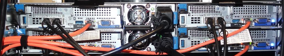
Are they running 2x 25Gbps NIC’s per server over standard cat 6? I thought 10Gbps over cat 6 was generally accepted as the fastest it can reliably push?
Is the 2/3 for caching using part of each NVMe, or is there one dedicated for the rest? Mostly wondering about spreading writes more evenly, rather than peak throughout.
• Image optimization is still mostly software: JPEG, PNG, WebP. GPUs do not bring much to the table here at all, and consume a lot of power, which is likely to upset the hosting ISP of that cache node.
• Video encoding is better, but still average. NVENC (Nvidia’s encode Engine) has some quality challenges and limitations.
Further, doing this at the edge makes less sense: if you have to fetch the source material from the origin, do the heavy lifting centrally and store the results at the edge. Storing 4-5 renditions is cheap compared to GPU running costs here.
In the last picture, the server seems to be 1U, but also squarish. Is there a benefit or a reason for not using the entire depth of the rack, or was there just nothing more to include?