> The operation itself [inside the dram module] actually requires 2x the power (20 pJ compared to 10 pJ [inside the main CPU]), but the overall gain in power efficiency is 170 pJ vs 3010 pJ, or just under 20x
> One thing that this slide states that might be confusing is the server power consumption – the regular server is listed as only 300W, but the PIM solution is up to 700W. This is because the power-per-DRAM module would increase under UPMEM’s solution.
I'm assuming that those numbers represent "peak" power, and that when idle the compute parts of the DRAM can be power/clock gated. The implication being that if you are doing lots of in-memory analytics, you'll get a power saving, but if you switch to "something else" and don't get good utilisation of the in-memory compute, you'll probably ruin your power/energy efficiency.
I guess that means the future improvements will involve bringing the power consumption of the modified DRAM modules back in line with their "normal" cousins.
Watts are Joules / second. If you're doing operations that take 1/20 as much power each but you're doing them 20x faster, it takes the same amount of power in Watts. For a better comparison you'd need to measure Watts * seconds for a given task.
Indeed, like how the best CPU reviews don't just report the power consumption but also the energy consumed to do a given benchmark (power integrated in time for a fixed amount of work).
skavi is right, in context I should have said that each operation takes 1/20 as much energy. The amount of power depends on how often the operations are done.
While it is very true that the memory is much bigger bottleneck than the CPU in computing today, it is a quite a bit disingenuous for the "in-memory" computing crowd to keep pointing to dramatic difference in energy needed for a memory transaction in "their vs ours" solution.
Yes, onchip SRAM can take single picojoules vs hundred picojules per bit on external DRAM, but using external DRAM is a perfectly valid design decision that does not dramatically increase the power consumption because CPUs have large caches and very smart prefetch logic. Some algorithms may seem to demand tens of gigabits of memory bandwidth on paper, but in reality smart prefetchers can reduce that to hundreds megabits.
Where things like this matters is scalability. Parallel computing performance scales not much with memory bandwidths per CPU, but with the number of individual CPUs, threads and their prefetch units. Here, the decision to have hundreds of wimpy CPUs, but all with individual memory access will be valid.
Prefetchers don't do anything do reduce the power consumption involved in streaming data from memory, they only reduce the latency seen by the CPU. In fact, since the prefetcher sometimes makes mispredictions, they tend to increase power.
But they do reduce cache misses and unneeded cache evictions dramatically, and that allows CPUs to use external memory less. This reduces the power consumption.
A prefetcher reduces cache misses by retrieving the data first; the number of memory accesses to get the data remains the same. [Though it may be through a more efficient pipelined operation].
How does a prefetcher reduce unneeded cache evictions? It fetches data that may not be needed, increasing cache evictions.
The only thing a prefetcher can do to improve power efficiency, IMO, is by increasing utilization-- if the processor stays 99% busy instead of 97% busy, the fixed portions of the power budget are amortized over more operations.
> A prefetcher reduces cache misses by retrieving the data first
I'm struggling with that. To avoid a cache miss the prefetcher woul have to prefetch the data from memory so early, and memory is so slow, that an entire train of in-flight instructions could complete, and then likely have the CPU pause, before the fetch-from-ram completed.
The whole point of a prefetcher is to avoid cache misses. What do you think a prefetcher is for?
Memory is very latent, and moderately slow. Hardware prefetching tends to mostly make memory accesses longer, so you don't pay the RAS/CAS penalties and instead stream just more memory words back to fill an additional cache line beyond the one demanded.
e.g. One key part of Intel L2 hardware prefetching is working upon cache line pairs. If you miss on an even numbered cache line, and counters support it, it decides to also retrieve the next odd-numbered cache line at the same time.
The downside of a hardware prefetcher is three things, both stemming from it perhaps retrieving memory that isn't needed. 1) it can cause useful information to be evicted from cache if a prefetch is errant. 2) it can tie up the memory bus with an unnecessary access and make a necessary one more latent. 3) it can consume power for a prefetch that isn't needed.
We may be talking past each other. My understanding of a prefetcher is to get the data ASAP. It typically prefetches from cache, not from memory (if it prefetches from mem it's so slow it's useless).
> Memory is very latent, and moderately slow
Those 2 terms seem synonymous, but memory access is slooow - from doc in front of me, for haswell:
for the ram latencies that's for different setups (single/dual cpu , I'm not sure) running ~3.5GHz. So for 36C + 57NS that 36 + (3.5 * 57) = 235 cycles latency. And it can get worse. Much worse.
I'm sorry i can't find it now but in hennesy & patterson I recall it being said that prefetchers can hide most of the latency of a L1 or L2 miss if it hits L3, but if it needs main mem then it's stuffed. Sorry, that is from memory and may be wrong! But I'm pretty sure a prefetcher is wasted if it needs to hit ram.
> If you miss on an even numbered cache line, and counters support it, it decides to also retrieve the next odd-numbered cache line at the same time.
I see, but I think it does better these days, it'll remember a stride and prefetch by the next stride. Even striding backwards through mem (cache)! But it won't cross a page boundary.
This is a DDR4 pipelined read timing diagram. The bank select and row select latencies are significant, "off the left of this diagram," and contribute to the latency of random reads.
Further sequential reads --- until we hit a boundary -- can continue with no interruption of output, and do not pay the latency penalty (because there's no further bank select and row select, and because the prefetch and memory controller logic strobed the new column address before the previous read completed).
> My understanding of a prefetcher is to get the data ASAP. It typically prefetches from cache, not from memory (if it prefetches from mem it's so slow it's useless).
The prefetcher runs at whatever level it's at (L1/L2) and fetches from whatever level has the memory. So the L2 prefetcher may be grabbing from L3, and may be grabbing from SDRAM.
That's the ram LATENCY ON RANDOM ACCESS. If you extend an access to fetch the next sequential line because you think it will be used, you don't pay any of the latency penalty-- you might need to strobe a column access but words keep streaming out. For this reason sequential prefetch is particularly powerful. Even if we're just retrieving from a single SDRAM channel, it's just another 3ns to continue on to retrieve the next line. (DDR4-2400 is 2400MT/s, 8 transactions to fill a line, 8/2400000000=3.3n)
> I see, but I think it does better these days, it'll remember a stride and prefetch by the next stride. Even striding backwards through mem (cache)! But it won't cross a page boundary.
Sure, the even/odd access extender is just one very simple prefetcher that is a part of modern intel processors that I included for illustration. And we're completely ignoring software prefetch.
Go ahead, do the experiment. Run a memory-heavy workload and look at cache miss rates. Then turn off prefetch and see what you get. Most workloads, you'll get a lot more misses. ;)
That thread is orthogonal, but what's there supports exactly what I'm saying: prefetch improves effective bandwidth to SDRAM at all layers.
A second, successive streamed fetch is basically free from a latency perspective. If you're missing, and have to go to memory, there's a very high chance that L2 is going to prefetch the next line into a stream buffer, and you won't miss to SDRAM next time.
It's reached the point that now that the stream prefetchers hint to the memory controller that a queued access is prefetch, so the memory controller can choose based on contention whether to service the prefetch or not.
Most of what you seem to talk about is L1 prefetch; I agree if L1 prefetch misses all the way to RAM you are probably screwed. The fancy strategies you mention, etc, are mostly L1 prefetch strategies. But L2 has its own prefetcher, and it's there to get rid of memory latency and increase effective use of memory bandwidth...
While we're talking about it... even the SDRAM itself has a prefetcher for burst access ;) Though it's kinda an abuse that it's called as such.
> How does a prefetcher reduce unneeded cache evictions? It fetches data that may not be needed, increasing cache evictions.
I wanted to say that a smarter prefetcher, or better to say a whole entirety of on-chip logic that works to minimise cache misses, will lower the rate of unneeded evictions.
> Some algorithms may seem to demand tenths of gigabits of memory bandwidth on paper, but in reality smart prefetchers can reduce that to hundred megabits.
Are tenths of a gigabit and hundreds of megabits not the same thing?
I'm glad to see that you mentioned this. I had the pleasure of working with Russell Fish on a different project, and I immediately thought of TOMI when looking at the parent article.
Seems to me that a full CPU is overkill for this; a hybrid approach where you just have some arithmetic on vectors, with no program counter or branching really, could be effective without adding a bunch of complexity.
Also seems like concurrency and data consistency issues could arise pretty drastically when each memory unit is potentially making changes independent of the processor...
> Internally the DPU uses an optimized 32-bit ISA with triadic instructions, with non-destructive operand compute. As mentioned, the optimized ISA contains a range of typical instructions that can easily be farmed out to in-memory compute, such as SHIFT+ADD/SHIFT+SUB, basic logic (NAND, NOR, ORN, ANDN, NXOR), shift and rotate instructions
The concept of "smart memory" is good (though not new), but I think the devil could be in the process-technology details; DRAM and logic are not that compatible.
First incarnations of this I heard of were SLAM, Scan Line Access Memory [1]
"A SLAM consists of a conventional dense semiconductor dynamic memory augmented with highly parallel, but simple, on-chip processors designed specifically for fast computer graphics rasterization. "
This sounds sketchy. Either the rest of the industry is incredibly incompetent or they are deliberately omitting a huge drawback of this solution. And I don't see lack of expandability as a drawback, just buy a bit more RAM to start with.
Then there are NVIDIA GPUs and Intel Phi (i.e. Knightslanding)... So they are trying to sell us that neither AMD, NVIDIA or Intel have though of this "ingenious" decision to increase the efficiency obtained by co-locating CPU and memory? The fact that they deliberately avoid addressing this elephant in the room makes me super skeptical.
It requires significant changes to the compiler, so this RAM would not make any difference to existing binaries. This is a really big change in the way computers are structured, so it's no wonder it hasn't taken off before. And this isn't the first attempt; look up computational RAM, IRAM, RADram, smart DRAM, processor-in-memory.
the drawback is the same as with all the others NUMA solution, the whole thing (mmu, os, code, controllers etc) needs to be aware of where the data comes and go because moving something from one bank to another stalls the compute pipeline for a lot, which makes compilers and thread scheduling and pagination etc a complex affair.
Not an expert here but the last time I got curious about the state of processor-in-memory my understanding was that the infeasibility of PIM is in large part due to mutually exclusive optimization paths in the fab processes used for CPUs verses for DRAM
So is any kind of disruption impossible then, if everything has already been thought of by other big players? The "big drawback" could be that it takes a big investment to try this, and it's a big risk as to whether that investment pays off.
Micron has been pursuing something similar for a while. The "CPUs" that you can put on the same die, however, are very limited in what they can do, owing to the specific lithography used on memory chips, and the general lack of die space. They also don't get uniform access to a huge memory range that you'd expect from a "real" CPU, and require you to partition work to fit within the constraints of the memory access pattern they can, in fact, support. The instruction set is very limited, floating point can only be emulated (i.e. slow AF, not that you actually need it for neural networks most of the time). The upside is the unlimited memory bandwidth and very low pJ/byte, with a few catches.
Don't know if this is similar, but if it is, it's going to be a hard sell, especially in the era when 90% of programmers can't even understand what I wrote above.
Interesting. The last I can find on the Automata Processor is from 2014, when it was supposedly being delivered to developers within weeks. And then nothing. I wonder what happened to it. Doesn't seem like it ever turned into a shipping product.
> This work was supported in part by the NSF (CCF-0954024, CCF-1116289, CDI-1124931, EF-1124931); Air Force (FA8750- 15-2-0075); Virginia Commonwealth Fellowship; Jefferson Scholars Foundation; the Virginia CIT CRCF program under grant no. MF14S-021-IT; by C-FAR, one of the six SRC STARnet Centers, sponsored by MARCO and DARPA; a grant from Micron Technology.
I remember reading about it at the times, needing to have support by the firmware/BIOS/UEFI when you wanted to plug this
into a system.
Seems it was too complicated, and got moved onto a pcie-card with fpga.
Makes me wonder if the automata rams as such are even produced, or they just bought Microns remainig stock, and go out of business if that runs out?
Wayback Machined captured statement from Micron, and where development continues:
"A blitter is a circuit, sometimes as a coprocessor or a logic block on a microprocessor, dedicated to the rapid movement and modification of data within a computer's memory."
As I recall there was "chip" ram and "fast" ram.
So maybe not embedded for all definitions but
certainly processing chips with privileged access
to a subset of memory
You have to obey speed of light latency, and that means putting compute in RAM right next to the data. Key is to have a reusable fabric so all the TSMC customers can pop their own chips in RAM, especially ASICS and micro-FPGAs.
Interesting that they went with a 32bit ISA, given the growth and demand for ML/AI, which seems to lean upon lower precision (8bit), then I wonder if they could of gone for that instead of something more a jack of all trades design.
Which makes me wonder, when will somebody do an ISA dedicated for ML/AI and will we ever see old 8bit CPU's reborn as on memory CPU's.
But we have seen this approach for processing upon memory before and whilst that has not tractioned into a product, this might. Though with Chip design going towards chiplets, ram can and may well become another chiplet in the evolution of that design process.
Since the processing elements seem to be unable to reach memory outside their own 64 MB block, 32 bit integers seem sufficient for pointers. Also, it has a 64-bit wide access to its memory block, but can't map it - all transfers are via DMA.
It must feel like a Cell processor with thousands of SPUs to play with.
The thing is, you still need 32-bit or 64-bit values for pointers, loop counters, etc. You're also going to want your CPU to interact and convert between richer data types. What you probably want is to have a 64-bit CPU and control unit, with some SIMD ALUs that operate on multiple 8-bit values at once.
Sidenote: I think that ML people are more interested in 16-bit floats than 8-bit integer values. Though none of that is mainstream yet, most ML code still uses 32-bit floating point numbers at the moment.
It's quite common to train at float32 but quantize down to int8 for inference. The loss of accuracy is negligible, but you make huge performance gains.
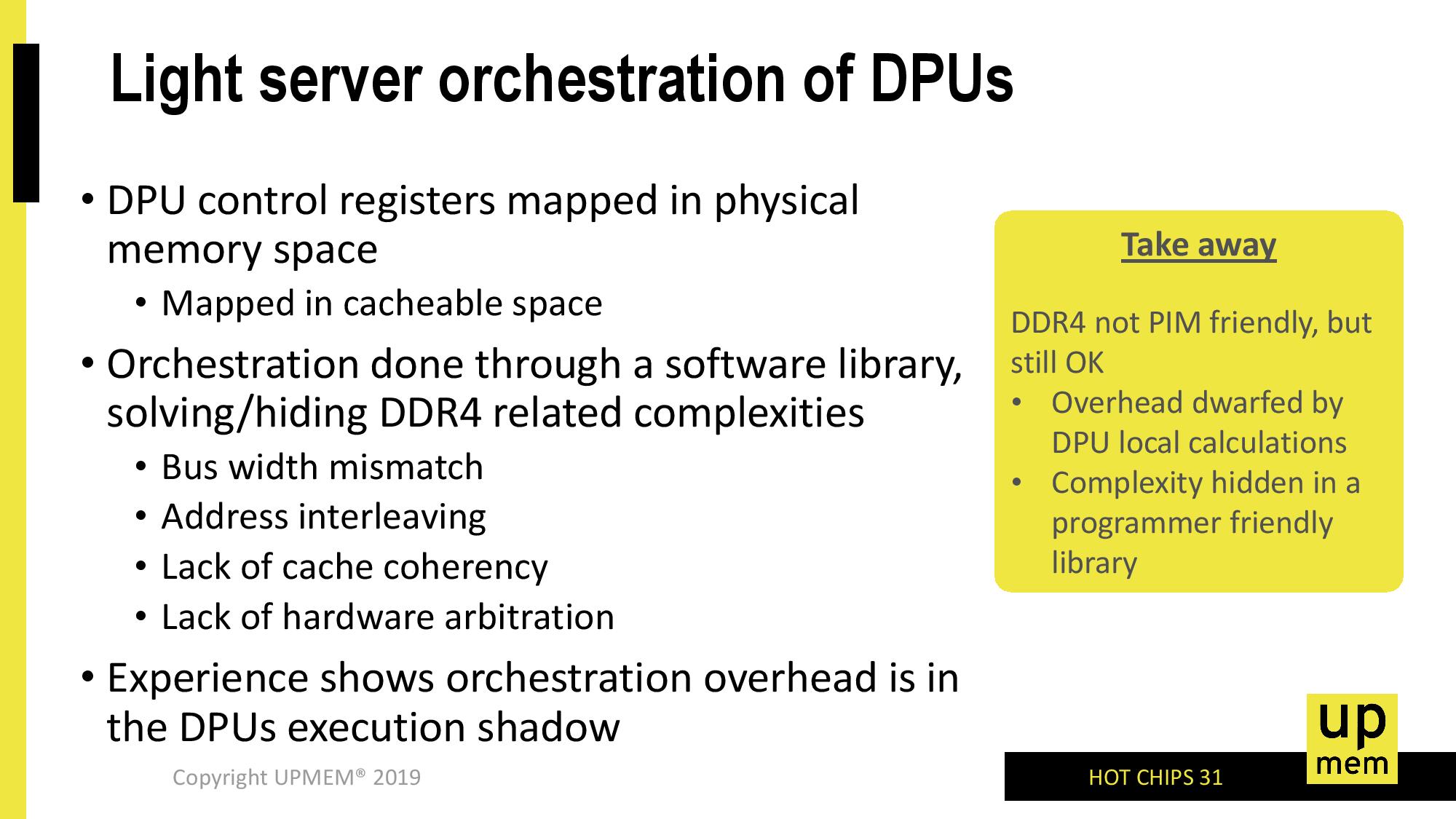
It seems you have to compile an executable for the in memory processor, and they have some sort of daemon/infrastructure to communicate from the main cpu to the PIM.
It can actually be useful for security - you can tell the DPUs to erase memory the moment the OS frees it, reducing the risk of data being read or decrypted. That's probably a very trivial use of the tech, but it's a low hanging fruit.
I suppose one could put more of an OS's work with memory into this level, too. Zero it when it's freed, but also keep the free block list updated at this level. Maybe use these processors for aggregating available contiguous blocks when necessary, too. Maybe use these processors to update the virtual to physical mappings and keep free space optimized. Then, when the application actually needs to do something close to RAM it could be given access.
I’m not much of a hardware person but I was wondering why not do the opposite? Pair a massive amount of SRAM/DRAM with a normal cpu as l2+ cache. Or is that what they are essentially doing?
20x speedup compared to a CPU looks worse than just using a stock GPU, and we haven't talked about the AI inference chips that are optimized for NN inferencing.
But they can prefetch data. This makes writing code for them a bit more complex, but outside of that the ram limitations are mostly moot.
This fails when data needs to be read and written randomly. However, even if the entire dataset was on vram random reads and writes would still be slow, because of the way a stream processor works. All reads and writes need to be laid out in memory in an order for a gpu to do it's best work.
I wonder what having these in-memory processing units can do with cryptocurrencies. Serial processing performance is rather low, but there are thousands of DPUs in a memory DIMM.
This is a great idea! I'm surprised we haven't thought of this before. Add a simple ALU in there with some request to perform some NN calculations like a co processor!
Integration and disaggregation of various parts of computer architecture is a constant cycle that depends on what’s the current bottleneck. For decades computers are connection of compute, memory, storage and network, and you can trade them based on what’s needed.
If transferring data is bottleneck, then companies start to integrate. But that has downside of not being able to grow resources at different speed, so once transferring data is no longer a bottleneck, everyone runs to disaggregate. And then it repeats.
A lot of current ideas were actually used in the past, but cycle phased them out, and they make a comeback right now.
Anandtech have an excellent analysis: https://www.anandtech.com/show/14750/hot-chips-31-analysis-i...
> The operation itself [inside the dram module] actually requires 2x the power (20 pJ compared to 10 pJ [inside the main CPU]), but the overall gain in power efficiency is 170 pJ vs 3010 pJ, or just under 20x
> One thing that this slide states that might be confusing is the server power consumption – the regular server is listed as only 300W, but the PIM solution is up to 700W. This is because the power-per-DRAM module would increase under UPMEM’s solution.
I'm assuming that those numbers represent "peak" power, and that when idle the compute parts of the DRAM can be power/clock gated. The implication being that if you are doing lots of in-memory analytics, you'll get a power saving, but if you switch to "something else" and don't get good utilisation of the in-memory compute, you'll probably ruin your power/energy efficiency.
I guess that means the future improvements will involve bringing the power consumption of the modified DRAM modules back in line with their "normal" cousins.